
Data Sheet

Si4702/03-C19
44 Rev. 1.1
DOCUMENT CHANGE LIST
Revision 0.8 to Revision 0.9
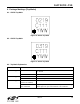
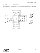
Updated Figure 1, “Reset Timing Parameters for
Busmode Select Method 1 (GPIO3 = 0),” on page 6.
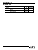
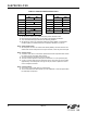
Updated Table 3, “DC Characteristics
1
,” on page 5.
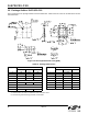
Updated Table 7, “2-Wire Control Interface
Characteristics
1,2,3
,” on page 10.
Updated Table 8, “FM Receiver Characteristics
1,2
,” on
page 12.
Updated 4.4. "RDS/RBDS Processor and
Functionality" on page 16.
Updated Register 1, “Chip ID,” on page 23.
Updated Register 5, “System Configuration 2,” on
page 28.
Revision 0.9 to Revision 1.0
Updated notes in Table 7 on page 10.
Updated Table 8 on page 12.
Updated “4. Functional Description”.
Updated “5. Register Summary”.
Updated “6. Register Descriptions”.
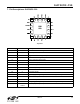
Updated “7. Pin Descriptions: Si4702/03-C19”.
Revision 1.0 to Revision 1.1
Updated Table 8 on page 12.
Updated “4.11. Initialization Sequence”.
Updated Register 06h: System Configuration 3.
Updated additional reference resources.