
Data Sheet

Si4702/03-C19
Rev. 1.1 21
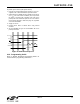
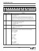
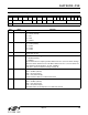
To power up the device (after power down):
1. Note that V
IO
is still supplied in this scenario. If V
IO
is not
supplied, refer to device initialization procedure above.
2. (Optional) Set the AHIZEN bit low to disable the dc bias of
0.5 x V
IO
volts at the LOUT and ROUT pins, but preserve
the states of the other bits in Register 07h. Note that in
powerup the LOUT and ROUT pins are set to the common
mode voltage specified in Table 8 on page 12, regardless
of the state of AHIZEN.
3. Supply V
A
and V
D
.
4. Provide RCLK. Refer to AN230 when using internal
oscillator.
5. Set the ENABLE bit high and the DISABLE bit low to
powerup the device.
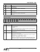
Figure 9. Initialization Sequence
4.12. Programming Guide
Refer to "AN230: Si4700/01 Programming Guide" for
control interface programming information.
VA,VD Supply
RCLK Pin
ENABLE Bit
1234
5
RST Pin
VIO Supply