
Data Sheet

Si4702/03-C19
20 Rev. 1.1
When proper voltages are applied to the
Si4702/03-C19, the ENABLE and DISABLE bits in
Register 02h can be used to select between powerup
and powerdown modes. When voltage is first applied to
the device, ENABLE = 0 and DISABLE = 0. Setting
ENABLE = 1 and DISABLE = 0 puts the device in
powerup mode. To power down the device, disable RDS
to prevent any unpredictable behavior (Si4703 only),
then write ENABLE and DISABLE bits to 1.
After being written to 1, both bits will be cleared as part
of the internal device powerdown sequence. To put the
device back into powerup mode, set ENABLE = 1 and
DISABLE = 0 as described above. The ENABLE bit
should never be written to a 0.
4.10. Audio Output Summation
The audio outputs LOUT and ROUT may be
capacitively summed with another device. Setting the
audio high-Z enable (AHIZEN) bit maintains a dc bias of
0.5 x V
IO
on the LOUT and ROUT pins to prevent the
ESD diodes from clamping to the V
IO
or GND rail in
response to the output swing of the other device. The
bias point is set with a 370 k resistor to V
IO
and GND.
Register 07h containing the AHIZEN bit must not be
written during the powerup sequence and only takes
effect when in powerdown and V
IO
is supplied. In
powerup the LOUT and ROUT pins are set to the
common mode voltage specified in Table 8, “FM
Receiver Characteristics
1,2
,” on page 12, regardless of
the state of AHIZEN. Bits 13:0 of register 07h must be
preserved as 0x0100 while in powerdown and as
0x3C04 while in powerup.
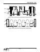
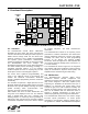
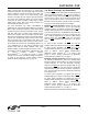
4.11. Initialization Sequence
Refer to Figure 9, “Initialization Sequence,” on page 21.
To initialize the device:
1. Supply V
A
and V
D
.
2. Supply V
IO
while keeping the RST pin low. Note that steps
1 and 2 may be reversed. Power supplies may be
sequenced in any order.
3. Select 2-wire or 3-wire control interface bus mode
operation as described in Section 4.9. "Reset, Powerup,
and Powerdown" on page 19.
4. Provide RCLK. Steps 3 and 4 may be reversed when using
an external oscillator. Refer to AN230 when using internal
oscillator.
5. Set the ENABLE bit high and the DISABLE bit low to
powerup the device. Software should wait for the powerup
time (as specified by Table 8, “FM Receiver
Characteristics
1,2
,” on page 12) before continuing with
normal part operation.
To power down the device:
1. (Optional) Set the AHIZEN bit high to maintain a dc bias of
0.5 x V
IO
volts at the LOUT and ROUT pins while in
powerdown, but preserve the states of the other bits in
Register 07h. Note that in powerup the LOUT and ROUT
pins are set to the common mode voltage specified in
Table 8 on page 12, regardless of the state of AHIZEN.
2. Set the ENABLE bit high and the DISABLE bit high to
place the device in powerdown mode. Note that all register
states are maintained so long as V
IO
is supplied and the
RST
pin is high.
3. (Optional) Remove RCLK.
4. Remove V
A
and V
D
supplies as needed.
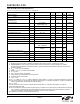
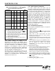
Table 9. Selecting 2-Wire or 3-Wire Control
Interface Busmode Operation
1,2,3
Busmode
Select Method
SEN SDIO GPIO1
GPIO3
2
Bus
mode
1 0 0 X 0
4
3-wire
1 1 0 X 0
4
2-wire
1
Xtal Oscillator
0 0 X 0
5
3-wire
1
Xtal Oscillator
1 0 X 0
5
2-wire
2 X X 0 1
6
3-wire
2 X X 1 1
6
2-wire
2
Xtal Oscillator
NA NA NA NA NA
2
Xtal Oscillator
NA NA NA NA NA
Notes:
1. All parameters applied on rising edge of RST.
2. When selecting 2-wire mode, the user must ensure
that SCLK is high during the rising edge of RST
, and
stays high until the 1st start condition.
3. GPIO3 is internally pulled down with a 1 M resistor.
4. GPIO3 should be externally driven low, set to high-Z
(10 M
or greater pull-up) or float.
5. GPIO3 should be left floating.
6. GPIO3 should be externally driven high (100 kor
smaller pull-up).