
Data Sheet

Si4702/03-C19
14 Rev. 1.1
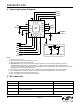
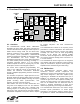
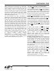
2. Typical Application Schematic
Notes:
1. Place C1 close to V
D
pin.
2. All grounds connect directly to GND plane on PCB.
3. Pins 1 and 20 are no connects, leave floating.
4. Important Note: FM Receiver performance is subject to adherence to antenna design guidelines in “AN231:
Si4700/01/02/03 Headphone and Antenna Interface.” Failure to use these guidelines will negatively affect the
performance of the Si4702/03-C19, particularly in weak signal and noisy environments. Silicon Laboratories will evaluate
schematics and layouts for qualified customers.
5. Pin 2 connects to the antenna interface, refer to “AN231: Si4700/01/02/03 Headphone and Antenna Interface.”
6. Place Si4702/03-C19 as close as possible to antenna jack and keep the FMIP trace as short as possible.
7. Refer to Si4702/03 Internal Crystal Oscillator Errata.
8. Refer to "AN299: External 32.768 kHz Crystal Oscillator."
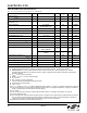
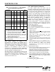
3. Bill of Materials
Component(s) Value/Description Supplier(s)
C1 Supply bypass capacitor, 22 nF, ±20%, Z5U/X7R Murata
U1 Si4702/03-C19 FM Radio Tuner Silicon Laboratories
C2, C3 Crystal load capacitors, 22 pF, ±5%, COG (Optional: for
crystal oscillator option)
Venkel
X1 32.768 kHz crystal (Optional: for crystal oscillator option) Epson
20
19
18
17
16
NC
FMIP
RFGND
GND
RST
GND
LOUT
ROUT
GND
VD
NC
GPIO1
GPIO2
GPIO3
VA
SEN
SCLK
SDIO
RCLK
VIO
SEN
SCLK
SDIO
1
2
3
4
5
15
14
13
12
11
6
7
8
9
10
RST
RCLK
C1
GND
PAD
LOUT
ROUT
VBATTERY
2.7 to 5.5 V
GPIO1
GPIO2
GPIO3
VIO
1.5 to 3.6 V
FMIP
RFGND
C2 C3
X1
RCLK
GPIO3
Optional: for crystal oscillator option