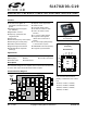
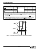
Si4702/03-C19 B RO A D C A S T F M R A DI O TU N E R FO R P O RTA BL E A PP L I C A T I O N S Features Ordering Information: See page 38. Pin Assignments (Top View) Pb-free/RoHS compliant RDS/RBDS Processor (Si4703) Integrated crystal oscillator Si4702/03-GM Applications Portable navigation Consumer electronics Description The Si4702/03 integrates the complete tuner function from antenna input to stereo audio output for FM broadcast radio reception.
Si4702/03-C19 2 Rev. 1.
Si4702/03-C19 TABLE O F C ONTENTS Section Page 1. Electrical Specifications . . . . . . . . . . . . . . . . . . . . . . . . . . . . . . . . . . . . . . . . . . . . . . . . . . .4 2. Typical Application Schematic . . . . . . . . . . . . . . . . . . . . . . . . . . . . . . . . . . . . . . . . . . . . . 14 3. Bill of Materials . . . . . . . . . . . . . . . . . . . . . . . . . . . . . . . . . . . . . . . . . . . . . . . . . . . . . . . . . . 14 4. Functional Description . . . . . . . . . . . . . . . . . . . .
Si4702/03-C19 1. Electrical Specifications Table 1. Recommended Operating Conditions Parameter Symbol Test Condition Min Typ Max Unit Digital Supply Voltage VD 2.7 — 5.5 V Analog Supply Voltage VA 2.7 — 5.5 V Interface Supply Voltage VIO 1.5 — 3.
Si4702/03-C19 Table 3. DC Characteristics1 (VD = VA = 2.7 to 3.6 V, VIO = 1.5 to 3.6 V, TA = –20 to 85 °C) Parameter Symbol Test Condition Min Typ Max Unit IA ENABLE = 1 — 10.8 — mA ID ENABLE = 1 — 3.3 — mA Interface Operating Supply Current2 IIO ENABLE = 1 — 0.3 — mA Total Operating Supply Current2,3,4,5 IOP ENABLE = 1 Low SNR signal — 15.3 16.8 mA Total Operating Supply Current2,3,4 IOP ENABLE = 1 — 14.4 15.
Si4702/03-C19 Table 4. Reset Timing Characteristics (Busmode Select Method 1)1,2,3 Parameter Symbol Test Condition Min Typ Max Unit RSTpulse width and GPIO3 Setup to RST tGSRST14 GPIO3 = 0 100 — — µs SEN and SDIO Setup to RST tSRST1 30 — — ns SEN, SDIO, and GPIO3 Hold from RST tHRST1 30 — — ns Notes: 1.
Si4702/03-C19 Table 5. Reset Timing Characteristics (Busmode Select Method 2)1,2,3 Parameter Symbol Test Condition Min Typ Max Unit GPIO1 and GPIO3 Setup to RST tSRST2 GPIO3 = 1 30 — — ns GPIO1 and GPIO3 Hold from RST tHRST2 30 — — ns Notes: 1. When selecting 2-wire Mode, the user must ensure that a 2-wire start condition (falling edge of SDIO while SCLK is high) does not occur within 300 ns before the rising edge of RST. 2.
Si4702/03-C19 Table 6. 3-Wire Control Interface Characteristics (VD = VA = 2.7 to 5.5 V, VIO = 1.5 to 3.6 V, TA = –20 to 85 °C) Parameter Symbol Test Condition Min Typ Max Unit SCLK Frequency fCLK 0 — 2.
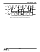
Si4702/03-C19 SCLK 70% SEN 70% 30% tHSDIO tS tCDV t HSEN1 tS tCDZ tHSEN2 30% 80% SDIO A7 20% A6-A5, R/W, A4-A1 Address In A0 D15 ½ Cycle Bus Turnaround D14-D1 D0 Data Out Figure 4. 3-Wire Control Interface Read Timing Parameters Rev. 1.
Si4702/03-C19 Table 7. 2-Wire Control Interface Characteristics1,2,3 (VD = VA = 2.7 to 5.5 V, VIO = 1.5 to 3.6 V, TA = –20 to 85 °C) Parameter Symbol Test Condition Min Typ Max Unit SCLK Frequency fSCL 0 — 400 kHz SCLK Low Time tLOW 1.3 — — µs SCLK High Time tHIGH 0.6 — — µs SCLK Input to SDIO Setup (START) tSU:STA 0.6 — — µs SCLK Input to SDIO Hold (START) tHD:STA 0.
Si4702/03-C19 SCLK 70% SDIO 70% tSU:STA tHD:STA tLOW START tr:IN tHIGH tr:IN tf:IN tSP tSU:STO tBUF 30% 30% tf:IN, tf:OUT tHD:DAT tSU:DAT STOP START Figure 5. 2-Wire Control Interface Read and Write Timing Parameters SCLK A6-A0, R/W SDIO START ADDRESS + R/W D7-D0 ACK DATA D7-D0 ACK DATA ACK STOP Figure 6. 2-Wire Control Interface Read and Write Timing Diagram Rev. 1.
Si4702/03-C19 Table 8. FM Receiver Characteristics1,2 (VD = VA = 2.7 to 5.5 V, VIO = 1.5 to 3.6 V, TA = –20 to 85 °C) Parameter Symbol Min Typ Max Unit 76 — 108 MHz (S+N)/N = 26 dB — 1.7 3.5 µVEMF Sensitivity (50 matching network)3,4,5,6,8 (S+N)/N = 26 dB — 1.
Si4702/03-C19 Table 8. FM Receiver Characteristics1,2 (Continued) (VD = VA = 2.7 to 5.5 V, VIO = 1.5 to 3.6 V, TA = –20 to 85 °C) Parameter Symbol Mono/Stereo Switching Level3,8,12 Test Condition Min Typ Max Unit BLNDADJ = 10 10 dB stereo separation — 34 — dBµVEMF 55 60 — dB — 58 — dB — 0.1 0.5 % DE = 0 70 75 80 µs Audio Mono S/N3,4,5,6,9 Audio Stereo S/N 3,5,6,8 BLNDADJ = 10 3,4,9,12 Audio THD De-emphasis Time Constant 13 DE = 1 45 50 54 µs 14 ENABLE = 1 0.
Si4702/03-C19 2. Typical Application Schematic GPIO1 19 GPIO1 18 GPIO2 17 GPIO3 16 VA NC 20 GPIO2 GPIO3 LOUT ROUT 7 SCLK 8 SDIO 9 RCLK 10 VIO GND PAD 15 GND 14 LOUT 13 ROUT 12 GND 11 VD 6 SEN FMIP RFGND 1 NC 2 FMIP 3 RFGND 4 GND 5 RST VBATTERY 2.7 to 5.5 V C1 RST SEN SCLK SDIO X1 GPIO3 C2 RCLK VIO 1.5 to 3.6 V RCLK C3 Optional: for crystal oscillator option Notes: 1. Place C1 close to VD pin. 2. All grounds connect directly to GND plane on PCB. 3.
Si4702/03-C19 4. Functional Description RFGND LNA PGA Q ADC AGC 0 / 90 DSP FILTER DEMOD MPX AUDIO LOW-IF DAC DAC GPIO 32.768 kHz ROUT GPIO VD AFC TUNE VA REG RDS (Si4703) XTAL OSC RSSI CONTROL INTERFACE VIO RCLK 2.7 - 5.5 V LOUT RST SDIO SCLK CONTROLLER I ADC FMIP AMPLIFIER Si4702/03 Headphone Cable SEN Figure 7. Si4702/03-C19 FM Receiver Block Diagram 4.1.
Si4702/03-C19 An image-reject mixer downconverts the RF signal to low-IF. The quadrature mixer output is amplified, filtered, and digitized with high resolution analog-to-digital converters (ADCs). This advanced architecture achieves superior performance by using digital signal processing (DSP) to perform channel selection, FM demodulation, and stereo audio processing compared to traditional analog architectures. 4.3. General Purpose I/O Pins The pins GPIO1–3 can serve multiple functions.
Si4702/03-C19 combine the stereo left and right audio channels to a mono (L+R) audio signal as the signal quality degrades to maintain optimum sound fidelity under varying reception conditions. The signal level range over which the stereo to mono blending occurs can be adjusted by setting the BLNDADJ[1:0] register. Stereo/mono status can be monitored with the ST register bit and mono operation can be forced with the MONO register bit.
Si4702/03-C19 For additional recommendations on optimizing the seek function, consult "AN284: Si4700/01/02/03 Seek Adjustability and Settings." 4.7. Reference Clock The Si4702/03-C19 accepts a 32.768 kHz reference clock to the RCLK pin. The reference clock is required whenever the ENABLE bit is set high. Refer to Table 3, “DC Characteristics1,” on page 5 for input switching voltage levels and Table 8, "FM Receiver Characteristics," on page 12 for frequency tolerance information.
Si4702/03-C19 writes, starting with the upper byte of register 02h, followed by the lower byte of register 02h, and onward until the lower byte of the last register is reached. The internal address counter then automatically wraps around to the upper byte of register 00h and proceeds from there until continuous writes end. Data transfer ends with the STOP condition (rising edge of SDIO while SCLK is high). After every STOP condition, the internal address counter is reset.
Si4702/03-C19 4.10. Audio Output Summation Table 9. Selecting 2-Wire or 3-Wire Control Interface Busmode Operation1,2,3 2 X X 1 16 2 Xtal Oscillator NA NA NA NA NA The audio outputs LOUT and ROUT may be capacitively summed with another device. Setting the audio high-Z enable (AHIZEN) bit maintains a dc bias of 0.5 x VIO on the LOUT and ROUT pins to prevent the ESD diodes from clamping to the VIO or GND rail in response to the output swing of the other device.
Si4702/03-C19 To power up the device (after power down): 1. Note that VIO is still supplied in this scenario. If VIO is not supplied, refer to device initialization procedure above. 2. (Optional) Set the AHIZEN bit low to disable the dc bias of 0.5 x VIO volts at the LOUT and ROUT pins, but preserve the states of the other bits in Register 07h. Note that in powerup the LOUT and ROUT pins are set to the common mode voltage specified in Table 8 on page 12, regardless of the state of AHIZEN. 3.
Rev. 1.
Si4702/03-C19 6. Register Descriptions Register 00h. Device ID Bit D15 D14 D13 D12 D11 D10 D9 D8 D7 D6 D5 Name PN[3:0] MFGID[11:0] Type R R D4 D3 D2 D1 D0 D4 D3 D2 D1 D0 Reset value = 0x1242 Bit Name Function 15:12 PN[3:0] Part Number. 0x01 = Si4702/03 11:0 MFGID[11:0] Manufacturer ID. 0x242 Register 01h.
Si4702/03-C19 Register 02h. Power Configuration Bit D15 D14 D13 D12 D11 Name DSMUTE DMUTE MONO Type R/W R/W R/W 0 R/W D10 D9 D8 RDSM SKMODE SEEKUP SEEK R/W R/W R/W R/W D7 D6 0 DISABLE R/W R/W D5 D4 D3 D2 D1 0 0 0 0 0 R/W R/W R/W R/W R/W D0 ENABLE R/W Reset value = 0x0000 Bit Name Function 15 DSMUTE 14 DMUTE Mute Disable. 0 = Mute enable (default). 1 = Mute disable. 13 MONO Mono Select. 0 = Stereo (default). 1 = Force mono.
Si4702/03-C19 Bit Name Function 7 Reserved Reserved. Always write to 0. 6 DISABLE Powerup Disable. Refer to “4.9. Reset, Powerup, and Powerdown”. Default = 0. 5:1 Reserved Reserved. Always write to 0. 0 ENABLE Powerup Enable. Refer to “4.9. Reset, Powerup, and Powerdown”. Default = 0. Register 03h.
Si4702/03-C19 Register 04h. System Configuration 1 Bit D15 D14 Name RDSIEN STCIEN Type R/W R/W D13 D12 D11 D10 D9 D8 D7 D6 D5 D4 D3 D2 D1 D0 0 RDS DE AGCD 0 0 BLNDADJ[1:0] GPIO3[1:0] GPIO2[1:0] GPIO1[1:0] R/W R/W R/W R/W R/W R/W R/W R/W R/W R/W Reset value = 0x0000 Bit Name Function 15 RDSIEN RDS Interrupt Enable. 0 = Disable Interrupt (default). 1 = Enable Interrupt.
Si4702/03-C19 Bit Name Function 3:2 GPIO2[1:0] General Purpose I/O 2. 00 = High impedance (default). 01 = STC/RDS interrupt. A logic high will be output unless an interrupt occurs as described below. 10 = Low. 11 = High. Setting STCIEN = 1 will generate a 5 ms low pulse on GPIO2 when the STC 0Ah[14] bit is set. Setting RDSIEN = 1 will generate a 5 ms low pulse on GPIO2 when the RDSR 0Ah[15] bit is set. 1:0 GPIO1[1:0] General Purpose I/O 1. 00 = High impedance (default). 01 = Reserved. 10 = Low.
Si4702/03-C19 Register 05h. System Configuration 2 Bit D15 D14 D13 D12 D11 Name SEEKTH[7:0] Type R/W D10 D9 D8 D7 D6 D5 D4 BAND[1:0] SPACE[1:0] R/W R/W D3 D2 D1 D0 VOLUME[3:0] R/W Reset value = 0x0000 Bit Name Function 15:8 SEEKTH[7:0] 7:6 BAND[1:0] Band Select. 00 = 87.5–108 MHz (USA, Europe) (Default). 01 = 76–108 MHz (Japan wide band). 10 = 76–90 MHz (Japan). 11 = Reserved. 5:4 SPACE[1:0] Channel Spacing. 00 = 200 kHz (USA, Australia) (default).
Si4702/03-C19 Register 06h. System Configuration 3 Bit D15 D14 D13 D12 Name SMUTER[1:0] SMUTEA[1:0] Type R/W R/W D11 D10 D9 D8 D7 D6 D5 D4 D3 D2 D1 0 0 0 VOLEXT SKSNR[3:0] SKCNT[3:0] R/W R/W R/W R/W R/W R/W D0 Reset value = 0x0000 Bit Name Function 15:14 SMUTER[1:0] Softmute Attack/Recover Rate. 00 = fastest (default). 01 = fast. 10 = slow. 11 = slowest. 13:12 SMUTEA[1:0] Softmute Attenuation. 00 = 16 dB (default). 01 = 14 dB. 10 = 12 dB. 11 = 10 dB.
Si4702/03-C19 Register 07h. Test 1 Bit D15 D14 D13 D12 D11 D10 D9 Name XOSCEN AHIZEN Type R/W D8 D7 D6 D5 D4 D3 D2 D1 D0 Reserved R/W R/W Reset value = 0x0100 Bit Name Function 15 XOSCEN Crystal Oscillator Enable. 0 = Disable (default). 1 = Enable. The internal crystal oscillator requires an external 32.768 kHz crystal as shown in 2. "Typical Application Schematic" on page 14.
Si4702/03-C19 Register 08h. Test 2 Bit D15 D14 D13 D12 D11 D10 D9 D8 Name Reserved Type R/W D7 D6 D5 D4 D3 D2 D1 D0 Reset value = 0x0000 Bit Name 15:0 Reserved Function Reserved. If written, these bits should be read first and then written with their pre-existing values. Do not write during powerup. Register 09h.
Si4702/03-C19 Register 0Ah. Status RSSI Bit D15 D14 D13 D12 D11 D10 D9 D8 D7 D6 D5 D4 D3 Name RDSR STC SF/BL AFCRL RDSS BLERA[1:0] ST RSSI[7:0] Type R R R R R R R R D2 D1 D0 Reset value = 0x0000 Bit Name 15 RDSR 14 STC Seek/Tune Complete. 0 = Not complete (default). 1 = Complete. The seek/tune complete flag is set when the seek or tune operation completes. Setting the SEEK 02h[8] or TUNE 03h[15] bit low will clear STC. 13 SF/BL Seek Fail/Band Limit. 0 = Seek successful.
Si4702/03-C19 Bit Name 8 ST 7:0 RSSI[7:0] Function Stereo Indicator. 0 = Mono. 1 = Stereo. Stereo indication is also available on GPIO3 by setting GPIO3 04h[5:4] = 01. RSSI (Received Signal Strength Indicator). RSSI is measured units of dBµV in 1 dB increments with a maximum of approximately 75 dBµV. Si4702/03-C19 does not report RSSI levels greater than 75 dBuV. Rev. 1.
Si4702/03-C19 Register 0Bh. Read Channel Bit D15 D14 D13 D12 D11 D10 D9 D8 Name BLERB[1:0] BLERC[1:0] BLERD[1:0] Type R R D7 D6 D5 D4 D3 D2 D1 D0 READCHAN[9:0] R R Reset value = 0x0000 Bit Name 15:14 BLERB[1:0] RDS Block B Errors. 00 = 0 errors requiring correction. 01 = 1–2 errors requiring correction. 10 = 3–5 errors requiring correction. 11 = 6+ errors or error in checkword, correction not possible. Available only in RDS Verbose mode (RDSM = 1). Refer to “4.4.
Si4702/03-C19 Register 0Ch. RDSA Bit D15 D14 D13 D12 D11 D10 D9 D8 D7 Name RDSA[15:0] Type R D6 D5 D4 D3 D2 D1 D0 D5 D4 D3 D2 D1 D0 Reset value = 0x0000 Bit Name 15:0 RDSA Function RDS Block A Data. Register 0Dh. RDSB Bit D15 D14 D13 D12 D11 D10 D9 D8 D7 Name RDSB[15:0] Type R D6 Reset value = 0x0000 Bit Name 15:0 RDSB Function RDS Block B Data. Rev. 1.
Si4702/03-C19 Register 0Eh. RDSC Bit D15 D14 D13 D12 D11 D10 D9 D8 D7 Name RDSC[15:0] Type R D6 D5 D4 D3 D2 D1 D0 D5 D4 D3 D2 D1 D0 Reset value = 0x0000 Bit Name 15:0 RDSC Function RDS Block C Data. Register 0Fh. RDSD Bit D15 D14 D13 D12 D11 D10 D9 D8 D7 Name RDSD[15:0] Type R D6 Reset value = 0x0000 Bit Name 15:0 RDSD 36 Function RDS Block D Data. Rev. 1.
Si4702/03-C19 5 VA RST GPIO3 4 17 16 15 GND 14 LOUT GND PAD 13 ROUT 12 GND 6 7 8 9 10 VIO GND GPIO2 3 18 RCLK RFGND GPIO1 2 19 SDIO FMIP 20 SCLK 1 SEN NC NC 7. Pin Descriptions: Si4702/03-C19 11 VD Top View Pin Number(s) Name 1, 20 NC 2 FMIP 3 RFGND 4, 12, 15, PAD GND Ground. Connect to ground plane on PCB. 5 RST Device reset input (active low). 6 SEN Serial enable input (active low). 7 SCLK Serial clock input. 8 SDIO Serial data input/output.
Si4702/03-C19 8. Ordering Guide Part Number* Package Type Operating Temperature Si4702-C19-GM Portable Broadcast Radio Tuner FM Stereo QFN Pb-free –20 to 85 °C Si4703-C19-GM Portable Broadcast Radio Tuner FM Stereo with RDS QFN Pb-free –20 to 85 °C Description *Note: Add an “(R)” at the end of the device part number to denote tape and reel option; 2500 quantity per reel. 38 Rev. 1.
Si4702/03-C19 9. Package Markings (Top Marks) 9.1. Si4702 Top Mark Figure 10. Si4702 Top Mark 9.2. Si4703 Top Mark Figure 11. Si4703 Top Mark 9.3. Top Mark Explanation Mark Method: YAG Laser Line 1 Marking: Part Number 02 = Si4702 03 = Si4703 Firmware Revision 19 = Firmware Revision 19 R = Die Revision C = Revision C Die TTT = Internal Code Internal tracking code. Line 2 Marking: Line 3 Marking: Circle = 0.
Si4702/03-C19 10. Package Outline: Si4702/03-C19 Figure 12 illustrates the package details for the Si4702/03-C19. Table 10 lists the values for the dimensions shown in the illustration. Figure 12. 20-Pin Quad Flat No-Lead (QFN) Table 10. Package Dimensions Symbol Millimeters Symbol Min Nom Max A 0.50 0.55 0.60 f A1 0.00 0.02 0.05 L 0.35 0.40 0.45 b 0.18 0.25 0.30 L1 0.00 — 0.10 c 0.27 0.32 0.37 aaa — — 0.10 bbb — — 0.10 ccc — — 0.08 ddd — — 0.10 eee — — 0.
Si4702/03-C19 11. PCB Land Pattern: Si4702/03-C19 Figure 13 illustrates the PCB land pattern details for the Si4702/03-C19. Table 11 lists the values for the dimensions shown in the illustration. Figure 13. PCB Land Pattern Rev. 1.
Si4702/03-C19 Table 11. PCB Land Pattern Dimensions Symbol Millimeters Min D D2 Symbol Max 2.71 REF 1.60 1.80 Min Max GE 2.10 — W — 0.34 — e 0.50 BSC X E 2.71 REF Y E2 f GD 1.60 1.80 2.53 BSC 2.10 Millimeters 0.28 0.61 REF ZE — 3.31 ZD — 3.31 — Notes: General 1. All dimensions shown are in millimeters (mm) unless otherwise noted. 2. Dimensioning and Tolerancing is per the ANSI Y14.5M-1994 specification. 3. This Land Pattern Design is based on IPC-SM-782 guidelines. 4.
Si4702/03-C19 ADDITIONAL REFERENCE RESOURCES AN230: Si4700/01/02/03 Programming Guide AN231: Si4700/01/02/03 Headphone and Antenna Interface Si4700/01/02/03 EVB User’s Guide AN234: Si4700/01/02/03 EVB Test Procedure AN235: Si4700/01/02/03 EVB Quick Start Guide AN243: Using RDS/RBDS with the Si4701/03 AN284: Si4700/01/02/03 Seek Adjustability and Settings AN299: External 32.
Si4702/03-C19 DOCUMENT CHANGE LIST Revision 0.8 to Revision 0.9 Updated Figure 1, “Reset Timing Parameters for Busmode Select Method 1 (GPIO3 = 0),” on page 6. Updated Table 3, “DC Characteristics1,” on page 5. Updated Table 7, “2-Wire Control Interface Characteristics1,2,3,” on page 10. Updated Table 8, “FM Receiver Characteristics1,2,” on page 12. Updated 4.4. "RDS/RBDS Processor and Functionality" on page 16. Updated Register 1, “Chip ID,” on page 23.
Si4702/03-C19 NOTES: Rev. 1.
Si4702/03-C19 CONTACT INFORMATION Silicon Laboratories Inc. 400 West Cesar Chavez Austin, Texas 78701 Tel:1+ (512) 416-8500 Fax:1+ (512) 416-9669 Toll Free:1+ (877) 444-3032 Email: FMinfo@silabs.com Internet: www.silabs.com The information in this document is believed to be accurate in all respects at the time of publication but is subject to change without notice.