
Data Sheet
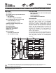

www.ti.com
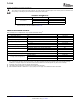
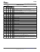
ELECTRICAL CHARACTERISTICS
TLC5940
SLVS515C – DECEMBER 2004 – REVISED OCTOBER 2007
V
CC
= 3 V to 5.5 V, T
A
= – 40 ° C to 85 ° C (unless otherwise noted)
PARAMETER TEST CONDITIONS MIN TYP MAX UNIT
V
OH
High-level output voltage I
OH
= -1mA, SOUT V
CC
– 0.5 V
V
OL
Low-level output voltage I
OL
= 1mA, SOUT 0.5 V
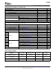
V
I
= V
CC
or GND; BLANK, DCPRG, GSCLK, SCLK, SIN,
– 1 1
XLAT
µ A
V
I
= GND; VPRG – 1 1
I
I
Input current
V
I
= V
CC
; VPRG 50
V
I
= 22V; VPRG; DCPRG = V
CC
4 10 mA
No data transfer, all output OFF,
0.9 6
V
O
= 1V, R
(IREF)
= 10k Ω
No data transfer, all output OFF,
5.2 12
V
O
= 1V, R
(IREF)
= 1.3k Ω
I
CC
Supply current mA
Data transfer 30MHz, all output ON,
16 25
V
O
= 1V, R
(IREF)
= 1.3k Ω
Data transfer 30MHz, all output ON,
30 60
V
O
= 1V, R
(IREF)
= 640 Ω
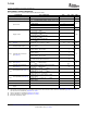
Constant sink current (see
I
O(LC)
All output ON, V
O
= 1V, R
(IREF)
= 640 Ω 54 61 69 mA
Figure 2 )
All output OFF, V
O
= 15V, R
(IREF)
= 640 Ω ,
I
lkg
Leakage output current 0.1 µ A
OUT0 to OUT15
All output ON, V
O
= 1V, R
(IREF)
= 640 Ω ,
1 ± 4
OUT0 to OUT15, – 20 ° C to 85 ° C
All output ON, V
O
= 1V, R
(IREF)
= 640 Ω ,
1 8
OUT0 to OUT15
(1)
Constant sink current error
Δ I
O(LC0)
%
(see Figure 2 )
All output ON, V
O
= 1V, R
(IREF)
= 320 Ω ,
1 6
OUT0 to OUT15, – 20 ° C to 85 ° C
All output ON, V
O
= 1V, R
(IREF)
= 320 Ω ,
± 1 ± 8
V
CC
= 4.5V to 5.5V, OUT0 to OUT15
(1)
– 2
Constant sink current error Device to device, Averaged current from OUT0 to
Δ I
O(LC1)
4 %
(see Figure 2 ) OUT15, R
(IREF)
= 1920 Ω (20mA)
(2)
+0.4
– 2.7
Constant sink current error Device to device, Averaged current from OUT0 to
Δ I
O(LC2)
± 4 %
(see Figure 2 ) OUT15, R
(IREF)
= 480 Ω (80mA)
(2)
+2
All output ON, V
O
= 1V, R
(IREF)
= 640 Ω
1 ± 4 %/V
OUT0 to OUT15, V
CC
= 3V to 5.5V
(3)
Δ I
O(LC3)
Line regulation (see Figure 2 )
All output ON, V
O
= 1V, R
(IREF)
= 320 Ω ,
± 1 ± 6 %/V
OUT0 to OUT15, V
CC
= 3V to 5.5V
(3)
All output ON, V
O
= 1V to 3V, R
(IREF)
= 640 Ω ,
± 2 ± 6 %/V
OUT0 to OUT15
(4)
Δ I
O(LC4)
Load regulation (see Figure 2 )
All output ON, V
O
= 1V to 3V, R
(IREF)
= 320 Ω ,
2 8 %/V
OUT0 to OUT15
(4)
T
(TEF)
Thermal error flag threshold Junction temperature
(5)
150 170 C
V
(LED)
LED open detection threshold 0.3 0.4 V
Reference voltage
V
(IREF)
R
(IREF)
= 640 Ω 1.20 1.24 1.28 V
output
(1) The deviation of each output from the average of OUT0-15 constant current. It is calculated by Equation 1 in Table 1 .
(2) The deviation of average of OUT1-15 constant current from the ideal constant-current value. It is calculated by Equation 2 in Table 1 .
The ideal current is calculated by Equation 3 in Table 1 .
(3) The line regulation is calculated by Equation 4 in Table 1 .
(4) The load regulation is calculated by Equation 5 in Table 1 .
(5) Not tested. Specified by design
4 Submit Documentation Feedback Copyright © 2004 – 2007, Texas Instruments Incorporated
Product Folder Link(s): TLC5940