
Data Sheet


www.ti.com
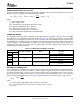
STATUS INFORMATION OUTPUT
LOD15
DC15.5
DC0.0 X
X
X
0
23
LODData
DCValues Reserved
MSB
LSB
119
120
24
TEF
LOD0 TEF
16
X
15
191
TLC5940
SLVS515C – DECEMBER 2004 – REVISED OCTOBER 2007
the grayscale register (see Figure 11 ). New grayscale data immediately becomes valid at the rising edge of the
XLAT signal; therefore, new grayscale data should be latched at the end of a grayscale cycle when BLANK is
high.The first GS data input cycle after dot correction requires an additional SCLK pulse after the XLAT signal to
complete the grayscale update cycle. All GS data in the input shift register is replaced with status information
data (SID) after updated the grayscale register.
The TLC5940 does have a status information register, which can be accessed in grayscale mode (VPRG=GND).
After the XLAT signal latches the data into the GS register the input shift register data will be replaced with status
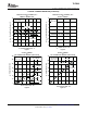
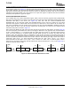
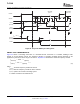
information data (SID) of the device (see Figure 18 ). LOD, TEF, and dot correction EEPROM data
(DCPRG=LOW) or dot correction register data (DCPRG=HIGH) can be read out at SOUT pin. The status
information data packet is 192 bits wide. Bits 0-15 contain the LOD status of each channel. Bit 16 contains the
TEF status. If DCPRG is low, bits 24-119 contain the data of the dot-correction EEPROM. If DCPRG is high, bits
24-119 contain the data of the dot-correction register.The remaining bits are reserved. The complete status
information data packet is shown in Figure 19 .
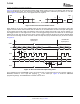
SOUT outputs the MSB of the SID at the same time the SID are stored in the SID register, as shown Figure 20 .
The next SCLK pulse, which will be the clock for receiving the SMB of the next grayscale data, transmits MSB-1
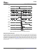
of SID. If output voltage is < 0.3 V (typical) when the output sink current turns on, LOD status flage becomes
active. The LOD status flag is an internal signal that pulls XERR pin down to low when the LOD status flag
becomes active. The delay time, tpd2 (1 µ s maximum), is from the time of turning on the output sink current to
the time LOD status flage becomes valid. The timing for each channel's LOD status to become valid is shifted by
the 30-ns (maximum) channel-to-channel turn-on time. After the first GSCLK goes high, OUT0 LOD status is
valid; tpd3 + tpd2 = 60 ns + 1 µ s. OUT1 LOD status is valid; tpd3 + td + tpd2 = 60 ns + 30 ns + 1 µ s = 1.09 µ s.
OUT2 LOD status is valid; tpd3 + 2*td + tpd2 = 1.12 µ s, and so on. It takes 1.51 µ s maximum (tpd3 + 15*td +
tpd2) from the first GSCLK rising edge until all LOD become valid; tsuLOD must be > 1.51 µ s (see Figure 20 ) to
ensure that all LOD data are valid.
Figure 19. Status Information Data Packet Format
18 Submit Documentation Feedback Copyright © 2004 – 2007, Texas Instruments Incorporated
Product Folder Link(s): TLC5940