
Data Sheet


www.ti.com
VPRG
DCPRG
XLAT
SIN
SCLK
SOUT
1
96
DC
MSB
-
DC
MSB
DC
LSB
VCC
V(PRG)
t
su6
t
prog
t
h5
DCPRG
OUT0
(Current)
t
pd5
t
pd5
OUT15
(Current)
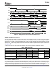
SETTING GRAYSCALE
Brightness in % +
GSn
4095
100
(9)
GS0.0
0
GS1.0
12
GS15.0
180
GS15.11
191
GS0.11
11
GS14.11
179
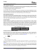
MSB LSB
GSOUT15 GSOUT0GSOUT14 − GSOUT2
TLC5940
SLVS515C – DECEMBER 2004 – REVISED OCTOBER 2007
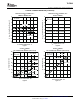
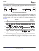
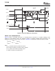
Figure 16. EEPROM Programming Timing Chart
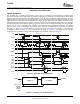
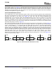
Figure 17. DCPRG and OUTn Timing Diagram
The TLC5940 can adjust the brightness of each channel OUTn using a PWM control scheme. The use of 12 bits
per channel results in 4096 different brightness steps, respective 0% to 100% brightness. Equation 9 determines
the brightness level for each output n:
where:
GSn = the programmed grayscale value for output n (GSn = 0 to 4095)
n = 0 to 15
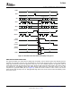
Grayscale data for all OUTn
Figure 18 shows the grayscale data packet format which consists of 12 bits x 16 channels, totaling 192 bits. The
format is Big-Endian format. This means that the MSB is transmitted first, followed by the MSB-1, etc.
Figure 18. Grayscale Data Packet Format
When VPRG is set to GND, the TLC5940 enters the grayscale data input mode. The device switches the input
shift register to 192-bit width. After all data is clocked in, a rising edge of the XLAT signal latches the data into
Copyright © 2004 – 2007, Texas Instruments Incorporated Submit Documentation Feedback 17
Product Folder Link(s): TLC5940