
Data Sheet


www.ti.com
DC0.0
0
DC1.0
6
DC15.0
90
DC15.5
95
DC0.5
5
DC14.5
89
MSB LSB
DCOUT15 DCOUT0
DCOUT14 − DCOUT2
t
su1
DCn
MSB
DCn
MSB−1
DCn
MSB−2
DCn
LSB+1
DCn
LSB
DCn
MSB
DCn+1
MSB
DCn+1
MSB−1
DCn
MSB−1
DCn
MSB−2
DCn−1
LSB
DCn−1
LSB+1
DCn−1
MSB
DCn−1
MSB−1
DCn−1
MSB−2
1 2 3 95 96 1 2
SCLK
SOUT
SIN
VPRG
XLAT
DCModeData
InputCyclen
DCModeData
InputCyclen+1
V
CC
t
wh0
t
wl0
DCn−1
LSB
t
wh2
t
h1
TLC5940
SLVS515C – DECEMBER 2004 – REVISED OCTOBER 2007
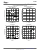
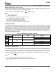
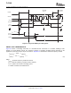
Figure 14 shows the dot correction data packet format which consists of 6 bits x 16 channel, total 96 bits. The
format is Big-Endian format. This means that the MSB is transmitted first, followed by the MSB-1, etc. The DC
15.5 in Figure 14 stands for the 5
th
most significant bit for output 15.
Figure 14. Dot Correction Data Packet Format
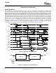
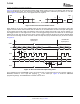
When VPRG is set to VCC, the TLC5940 enters the dot correction data input mode. The length of input shift
register becomes 96 bits. After all serial data are shifted in, the TLC5940 writes the data in the input shift register
to DC register when XLAT is high, and holds the data in the DC register when XLAT is low. The DC register is a
level triggered latch of XLAT signal. Since XLAT is a level-triggered signal, SCLK and SIN must not be changed
while XLAT is high. After XLAT goes low, data in the DC register is latched and does not change. BLANK signal
does not need to be high to latch in new data. XLAT has setup time (tsu1) and hold time (th1) to SCLK as shown
in Figure 15 .
Figure 15. Dot Correction Data Input Timing Chart
The TLC5940 also has an EEPROM to store dot correction data. To store data from the dot correction register to
EEPROM, DCPRG is set to high after applying V
PRG
to the VPRG pin. Figure 16 shows the EEPROM
programming timings. The EEPROM has a default value of all 1s.
16 Submit Documentation Feedback Copyright © 2004 – 2007, Texas Instruments Incorporated
Product Folder Link(s): TLC5940