
Data Sheet


www.ti.com
PRINCIPLES OF OPERATION
SERIAL INTERFACE
VPRG
XLAT
SIN
SCLK
SOUT
BLANK
GSCLK
OUT0
(current)
OUT1
(current)
OUT15
(current)
XERR
1
96
DC
MSB
DC
LSB
DC
MSB
1 192
193
1
192
193
1
1 4096
t
su4
t
h4
t
wh3
1
GS1
MSB
GS1
LSB
GS1
MSB
GS2
MSB
GS2
LSB
GS2
MSB
SID2
MSB
SID2
MSB-1
SID1
MSB
SID1
MSB-1
SID1
LSB
GS3
MSB
- --
t
wh2
t
su2
t
su1
t
wh0
t
wl0
t
su0
t
h0
t
pd0
t
pd1
t +t
pd1 d
t +15xt
pd1 d
t
pd3
t
d
15xt
d
t
pd2
t +t
pd3 d
t
pd3
t
pd4
t
wl1
t
wh1
DCDataInputMode
GSDataInputMode
1stGSDataInputCycle
2ndGSDataInputCycle
1stGSDataOutputCycle 2ndGSDataOutputCycle
t
su3
t
h3
t
h2
t
h1
t
su5
T
gsclk
t
outon
SIN
SOUT
SIN(a) SOUT(b)
TLC5940(a)
GSCLK,
BLANK,
SIN
SOUT
TLC5940(b)
SCLK,XLAT,
VPRG
DCPRG,
TLC5940
SLVS515C – DECEMBER 2004 – REVISED OCTOBER 2007
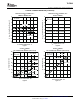
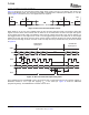
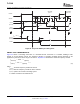
The TLC5940 has a flexible serial interface, which can be connected to microcontrollers or digital signal
processors in various ways. Only 3 pins are needed to input data into the device. The rising edge of SCLK signal
shifts the data from the SIN pin to the internal register. After all data is clocked in, a high-level pulse of XLAT
signal latches the serial data to the internal registers. The internal registers are level-triggered latches of XLAT
signal. All data are clocked in with the MSB first. The length of serial data is 96 bit or 192 bit, depending on the
programming mode. Grayscale data and dot correction data can be entered during a grayscale cycle. Although
new grayscale data can be clocked in during a grayscale cycle, the XLAT signal should only latch the grayscale
data at the end of the grayscale cycle. Latching in new grayscale data immediately overwrites the existing
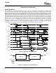
grayscale data. Figure 11 shows the timing chart. More than two TLC5940s can be connected in series by
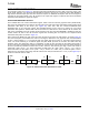
connecting an SOUT pin from one device to the SIN pin of the next device. An example of cascading two
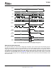
TLC5940s is shown in Figure 12 and the timing chart is shown in Figure 13 . The SOUT pin can also be
connected to the controller to receive status information from TLC5940 as shown in Figure 22 .
Figure 11. Serial Data Input Timing Chart
Figure 12. Cascading Two TLC5940 Devices
12 Submit Documentation Feedback Copyright © 2004 – 2007, Texas Instruments Incorporated
Product Folder Link(s): TLC5940