
Data Sheet

MMA8452Q
Sensors
8 Freescale Semiconductor, Inc.
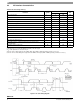
2.3 I
2
C interface characteristics
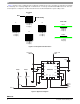
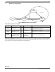
Figure 5. I
2
C slave timing diagram
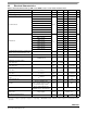
Table 4. I
2
C slave timing values
(1)
1.All values referred to V
IH(min)
(0.3V
DD
) and V
IL(max)
(0.7V
DD
) levels.
Parameter Symbol
I
2
C Fast Mode
Unit
Min Max
SCL clock frequency f
SCL
0 400 kHz
Bus-free time between STOP and START condition t
BUF
1.3 μs
(Repeated) START hold time t
HD;STA
0.6 μs
Repeated START setup time t
SU;STA
0.6 μs
STOP condition setup time t
SU;STO
0.6 μs
SDA data hold time t
HD;DAT
0.05 0.9
(2)
2.This device does not stretch the LOW period (t
LOW
) of the SCL signal.
μs
SDA setup time t
SU;DAT
100 ns
SCL clock low time t
LOW
1.3 μs
SCL clock high time t
HIGH
0.6 μs
SDA and SCL rise time t
r
20 + 0.1 C
b
(3)
3.C
b
= total capacitance of one bus line in pF.
300 ns
SDA and SCL fall time t
f
20 + 0.1 C
b
(3)
300 ns
SDA valid time
(4)
4.t
VD;DAT
= time for data signal from SCL LOW to SDA output (HIGH or LOW, depending on which one is worse).
t
VD;DAT
0.9
(2)
μs
SDA valid acknowledge time
(5)
5.t
VD;ACK
= time for Acknowledgement signal from SCL LOW to SDA output (HIGH or LOW, depending on which one is worse).
t
VD;ACK
0.9
(2)
μs
Pulse width of spikes on SDA and SCL that must be suppressed by
internal input filter
t
SP
050ns
Capacitive load for each bus line Cb 400 pF
V
IL
= 0.3V
DD
V
IH
= 0.7V
DD