
Data Sheet
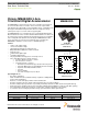

MMA8452Q
Sensors
Freescale Semiconductor, Inc. 5
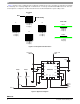
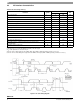
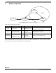
The device power is supplied through VDD line. Power supply decoupling capacitors (100 nF ceramic plus 4.7 µF bulk, or a
single 4.7 µF ceramic) should be placed as near as possible to the pins 1 and 14 of the device.
The control signals SCL, SDA, and SA0 are not tolerant of voltages more than VDDIO + 0.3V. If VDDIO is removed, the control
signals SCL, SDA, and SA0 will clamp any logic signals with their internal ESD protection diodes.
The functions, the threshold and the timing of the two interrupt pins (INT1 and INT2) are user programmable through the I
2
C
interface. The SDA and SCL I
2
C connections are open drain and therefore require a pullup resistor as shown in the application
diagram in Figure 4.
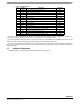
1.1 Soldering Information
The QFN package is compliant with the RoHS standard. Please refer to AN4077.
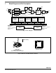
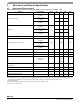
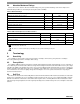
Table 1. Pin Descriptions
Pin # Pin Name Description Pin Status
1 VDDIO
Power Supply for IO pins (1.62V - 3.6V)
Input
2BYP
Bypass capacitor (0.1 μF)
Input
3NC
Leave open. Do not connect.
Open
4SCL
I
2
C Serial Clock
Open Drain
5GND
Connect to Ground
Input
6SDA
I
2
C Serial Data
Open Drain
7 SA0
I
2
C Least Significant Bit of the Device I
2
C Address
Input
8NC
Internally not connected (can be GND or VDD)
Input
9INT2
Inertial Interrupt 2
Output
10 GND
Connect to Ground
Input
11 INT1
Inertial Interrupt 1
Output
12 GND
Connect to Ground
Input
13 NC
Internally not connected (can be GND or VDD)
Input
14 VDD
Internal Power Supply (1.95V to 3.6V)
Input
15 NC
Internally not connected (can be GND or VDD)
Input
16 NC
Internally not connected (can be GND or VDD)
Input