
Data Sheet

Register description H3LIS331DL
28/38 DocID023111 Rev 3
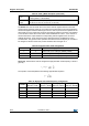
The BDU bit is used to inhibit output register updates between the reading of upper and
lower register parts. In default mode (BDU = ‘0’), the lower and upper register parts are
updated continuously. When the BDU is activated (BDU = ‘1’), the content of the output
registers is not updated until both MSB and LSB are read which avoids reading values
related to different sample times.
7.6 CTRL_REG5 (24h)
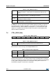
Turn-on bits are used for turning on the sleep-to-wake function.
Setting TurnOn[1:0] bits to 11, the “sleep-to-wake” function is enabled. When an interrupt
event occurs, the device is turned to normal mode, increasing the ODR to the value defined
in CTRL_REG1. Although the device is in normal mode, CTRL_REG1 content is not
automatically changed to “normal mode” configuration.
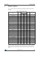
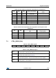
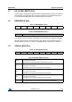
Table 29. CTRL_REG4 description
BDU
Block data update. Default value: 0
(0: continuous update; 1: output registers not updated between MSB and LSB
reading)
BLE
Big/little endian data selection. Default value 0.
(0: data LSB @ lower address; 1: data MSB @ lower address)
FS1, FS0
Full scale selection. Default value: 00.
(00: ±100 g; 01: ±200 g; 11: ±400 g)
SIM
SPI serial interface mode selection. Default value: 0.
(0: 4-wire interface; 1: 3-wire interface)
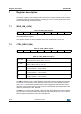
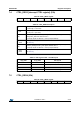
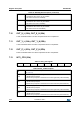
Table 30. CTRL_REG5 register
0 0 0 0 0 0 TurnOn1 TurnOn0
Table 31. CTRL_REG5 description
TurnOn1,
TurnOn0
Turn-on mode selection for sleep-to-wake function. Default value: 00.
Table 32. Sleep-to-wake configuration
TurnOn1 TurnOn0 Sleep-to-wake status
0 0 Sleep-to-wake function is disabled
11
Turned on: The device is in low-power mode (ODR is defined in
CTRL_REG1)