
Data Sheet


DocID023111 Rev 3 17/38
H3LIS331DL Digital interfaces
38
5 Digital interfaces
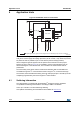
The registers embedded inside the H3LIS331DL may be accessed through both the I
2
C and
SPI serial interfaces. The latter may be SW configured to operate either in 3-wire or 4-wire
interface mode.
The serial interfaces are mapped onto the same pads. To select/exploit the I
2
C interface, the
CS line must be tied high (i.e. connected to Vdd_IO).
5.1 I
2
C serial interface
The H3LIS331DL I
2
C is a bus slave. The I
2
C is employed to write data into registers whose
content can also be read back.
The relevant I
2
C terminology is given in the table below.
There are two signals associated with the I
2
C bus: the serial clock line (SCL) and the serial
data line (SDA). The latter is a bi-directional line used for sending and receiving the data
to/from the interface. Both the lines are connected to Vdd_IO through a pull-up resistor
embedded inside the H3LIS331DL. When the bus is free both lines are high.
The I
2
C interface is compliant with fast mode (400 kHz) I
2
C standards as well as with
normal mode.
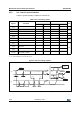
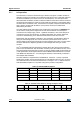
Table 8. Serial interface pin description
Pin name Pin description
CS
SPI enable
I
2
C/SPI mode selection (1: I
2
C mode; 0: SPI enabled)
SCL
SPC
I
2
C serial clock (SCL)
SPI serial port clock (SPC)
SDA
SDI
SDO
I
2
C serial data (SDA)
SPI serial data input (SDI)
3-wire interface serial data output (SDO)
SA0
SDO
I
2
C less significant bit of the device address (SA0)
SPI serial data output (SDO)
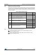
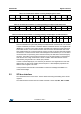
Table 9. Serial interface pin description
Term Description
Transmitter The device which sends data to the bus
Receiver The device which receives data from the bus
Master
The device which initiates a transfer, generates clock signals and terminates a
transfer
Slave The device addressed by the master