
Data Sheet


Application hints H3LIS331DL
16/38 DocID023111 Rev 3
4 Application hints
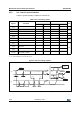
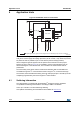
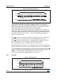
Figure 5. H3LIS331DL electrical connections
The device core is supplied through the Vdd line while the I/O pads are supplied through the
Vdd_IO line. Power supply decoupling capacitors (100 nF ceramic, 10 μF aluminum) should
be placed as near as possible to pin 14 of the device (common design practice).
All the voltage and ground supplies must be present at the same time to have proper
behavior of the IC (refer to Figure 5). It is possible to remove Vdd maintaining Vdd_IO
without blocking the communication bus, in this condition the measurement chain is
powered off.
The functionality of the device and the measured acceleration data are selectable and
accessible through the I
2
C or SPI interfaces. When using the I
2
C, CS must be tied high.
The functions, the threshold and the timing of the two interrupt pins (INT 1 and INT 2) can be
completely programmed by the user through the I
2
C/SPI interface.
4.1 Soldering information
The LGA package is compliant with the ECOPACK
®
, RoHS and “Green” standards.
It is qualified for soldering heat resistance according to JEDEC J-STD-020C.
Leave “pin 1 indicator” unconnected during soldering.
Land pattern and soldering recommendations are available at www.st.com.
CS
10µF
Vdd
100nF
GND
Vdd_IO
SDO/SA0
SDA/SDI/SDO
INT 1
SCL/SPC
Digital signal from/to signal controller. Signal levels are defined by proper selection of Vdd_IO
1
5
8
13
TOP VIEW
6
9
1416
9
5
INT 2
AM12626V1