
Data Sheet


Mechanical and electrical specifications H3LIS331DL
12/38 DocID023111 Rev 3
2.3.2 I
2
C - inter-IC control interface
Subject to general operating conditions for Vdd and Top.
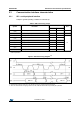
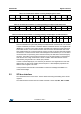
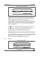
Figure 4. I
2
C slave timing diagram
Note: Measurement points are done at 0.2·Vdd_IO and 0.8·Vdd_IO, for both ports.
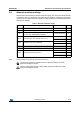
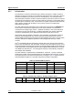
Table 6. I
2
C slave timing values
Symbol Parameter
I
2
C standard mode
(1)
I
2
C fast mode
(1)
Unit
Min. Max. Min. Max.
f
(SCL)
SCL clock frequency 0 100 0 400 KHz
t
w(SCLL)
SCL clock low time 4.7 1.3
μs
t
w(SCLH)
SCL clock high time 4.0 0.6
t
su(SDA)
SDA setup time 250 100 ns
t
h(SDA)
SDA data hold time 0.01 3.45 0.01 0.9 μs
t
r(SDA)
t
r(SCL)
SDA and SCL rise time 1000 20 + 0.1C
b
(2)
300
ns
t
f(SDA)
t
f(SCL)
SDA and SCL fall time 300 20 + 0.1C
b
(2)
300
t
h(ST)
START condition hold time 4 0.6
μs
t
su(SR)
Repeated START condition
setup time
4.7 0.6
t
su(SP)
STOP condition setup time 4 0.6
t
w(SP:SR)
Bus free time between STOP
and START condition
4.7 1.3
1. Data based on standard I
2
C protocol requirement, not tested in production.
2. C
b
= total capacitance of one bus line, in pF.
SD A
SCL
t
f(SD A )
t
su (SP)
t
w(SC LL)
t
su (SD A )
t
r(SD A )
t
su (SR)
t
h(ST)
t
w(SC LH )
t
h(SD A )
t
r(SCL)
t
f(SCL)
t
w(SP:SR)
START
REPEA TED
STA RT
STO P
STA RT