H3LIS331DL MEMS motion sensor: low-power high-g 3-axis digital accelerometer Datasheet - production data Description The H3LIS331DL is a low-power highperformance 3-axis linear accelerometer belonging to the “nano” family, with digital I2C/SPI serial interface standard output. The device features ultra-low power operational modes that allow advanced power saving and smart sleep-to-wakeup functions. TFLGA 3x3x1.
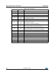
Contents H3LIS331DL Contents 1 2 3 4 Block diagram and pin description . . . . . . . . . . . . . . . . . . . . . . . . . . . . . 7 1.1 Block diagram . . . . . . . . . . . . . . . . . . . . . . . . . . . . . . . . . . . . . . . . . . . . . . . 7 1.2 Pin description . . . . . . . . . . . . . . . . . . . . . . . . . . . . . . . . . . . . . . . . . . . . . . 7 Mechanical and electrical specifications . . . . . . . . . . . . . . . . . . . . . . . . 9 2.1 Mechanical characteristics . . . . . . . . . .
H3LIS331DL 7 Contents Register description . . . . . . . . . . . . . . . . . . . . . . . . . . . . . . . . . . . . . . . . 24 7.1 WHO_AM_I (0Fh) . . . . . . . . . . . . . . . . . . . . . . . . . . . . . . . . . . . . . . . . . . . 24 7.2 CTRL_REG1 (20h) . . . . . . . . . . . . . . . . . . . . . . . . . . . . . . . . . . . . . . . . . . 24 7.3 CTRL_REG2 (21h) . . . . . . . . . . . . . . . . . . . . . . . . . . . . . . . . . . . . . . . . . . 25 7.4 CTRL_REG3 [interrupt CTRL register] (22h) . . . .
List of tables H3LIS331DL List of tables Table 1. Table 2. Table 3. Table 4. Table 5. Table 6. Table 7. Table 8. Table 9. Table 10. Table 11. Table 12. Table 13. Table 14. Table 15. Table 16. Table 17. Table 18. Table 19. Table 20. Table 21. Table 22. Table 23. Table 24. Table 25. Table 26. Table 27. Table 28. Table 29. Table 30. Table 31. Table 32. Table 33. Table 34. Table 35. Table 36. Table 37. Table 38. Table 39. Table 40. Table 41. Table 42. Table 43. Table 44. Table 45. Table 46. Table 47.
H3LIS331DL Table 49. Table 50. Table 51. Table 52. Table 53. Table 54. Table 55. Table 56. List of tables INT2_SRC register . . . . . . . . . . . . . . . . . . . . . . . . . . . . . . . . . . . . . . . . . . . . . . . . . . . . . . . 33 INT2_SRC description . . . . . . . . . . . . . . . . . . . . . . . . . . . . . . . . . . . . . . . . . . . . . . . . . . . . 33 INT2_THS register . . . . . . . . . . . . . . . . . . . . . . . . . . . . . . . . . . . . . . . . . . . . . . . . . . . . . . .
List of figures H3LIS331DL List of figures Figure 1. Figure 2. Figure 3. Figure 4. Figure 5. Figure 6. Figure 7. Figure 8. Figure 9. Figure 10. Figure 11. Figure 12. 6/38 Block diagram . . . . . . . . . . . . . . . . . . . . . . . . . . . . . . . . . . . . . . . . . . . . . . . . . . . . . . . . . . . . 7 Pin connections . . . . . . . . . . . . . . . . . . . . . . . . . . . . . . . . . . . . . . . . . . . . . . . . . . . . . . . . . . 7 SPI slave timing diagram (2) . . . . . . . . . . . . . . . . . . .
H3LIS331DL Block diagram and pin description 1 Block diagram and pin description 1.1 Block diagram Figure 1. Block diagram X+ Y+ CHARGE AMPLIFIER Z+ a CS I2C A/D CONVERTER MUX CONTROL LOGIC SCL/SPC SDA/SDO/SDI SPI Z- SDO/SA0 YX- TRIMMING CIRCUITS REFERENCE CONTROL LOGIC CLOCK INT 1 & INTERRUPT GEN. INT 2 AM12624V1 1.2 Pin description Figure 2.
Block diagram and pin description H3LIS331DL Table 2.
H3LIS331DL Mechanical and electrical specifications 2 Mechanical and electrical specifications 2.1 Mechanical characteristics @ Vdd = 2.5 V, T = 25 °C unless otherwise noted (a). Table 3. Mechanical characteristics Symbol FS So Parameter Test conditions (2) Measurement range Sensitivity(3) Min. Typ.
Mechanical and electrical specifications 2.2 H3LIS331DL Electrical characteristics @ Vdd = 2.5 V, T = 25 °C unless otherwise noted (b). Table 4. Electrical characteristics Symbol Vdd Vdd_IO Parameter Test conditions Supply voltage (2) I/O pins supply voltage Min. Typ.(1) Max. Unit 2.16 2.5 3.6 V Vdd+0.1 V 1.
H3LIS331DL Mechanical and electrical specifications 2.3 Communication interface characteristics 2.3.1 SPI - serial peripheral interface Subject to general operating conditions for Vdd and Top. Table 5. SPI slave timing values Value (1) Symbol Parameter Unit Min.
Mechanical and electrical specifications H3LIS331DL I2C - inter-IC control interface 2.3.2 Subject to general operating conditions for Vdd and Top. Table 6. I2C slave timing values Symbol I2C standard mode (1) Parameter f(SCL) SCL clock frequency I2C fast mode (1) Min. Max. Min. Max. 0 100 0 400 tw(SCLL) SCL clock low time 4.7 1.3 tw(SCLH) SCL clock high time 4.0 0.6 tsu(SDA) SDA setup time 250 100 th(SDA) SDA data hold time 0.01 ns 0.01 0.
H3LIS331DL 2.4 Mechanical and electrical specifications Absolute maximum ratings Stresses above those listed as “absolute maximum ratings” may cause permanent damage to the device. This is a stress rating only and functional operation of the device under these conditions is not implied. Exposure to maximum rating conditions for extended periods may affect device reliability. Table 7. Absolute maximum ratings Symbol Vdd Vdd_IO Vin Maximum value Unit Supply voltage -0.3 to 4.
Mechanical and electrical specifications 2.5 Terminology 2.5.1 Sensitivity H3LIS331DL Sensitivity describes the gain of the sensor and can be determined by applying 1 g acceleration to it. As the sensor can measure DC accelerations this can be done easily by pointing the axis of interest towards the center of the Earth, noting the output value, rotating the sensor by 180 degrees (pointing to the sky) and noting the output value again. By doing so, ±1 g acceleration is applied to the sensor.
H3LIS331DL 3 Functionality Functionality The H3LIS331DL is a “nano”, low-power, digital output 3-axis linear accelerometer housed in an LGA package. The complete device includes a sensing element and an IC interface able to take the information from the sensing element and to provide a signal to the external world through an I2C/SPI serial interface. 3.1 Sensing element A proprietary process is used to create a surface micromachined accelerometer.
Application hints 4 H3LIS331DL Application hints Figure 5. H3LIS331DL electrical connections Vdd 16 10µF 14 1 Vdd_IO 13 TOP VIEW INT 1 100nF 9 5 SDO/SA0 SDA/SDI/SDO SCL/SPC INT 2 CS 8 6 GND Digital signal from/to signal controller. Signal levels are defined by proper selection of Vdd_IO AM12626V1 The device core is supplied through the Vdd line while the I/O pads are supplied through the Vdd_IO line.
H3LIS331DL 5 Digital interfaces Digital interfaces The registers embedded inside the H3LIS331DL may be accessed through both the I2C and SPI serial interfaces. The latter may be SW configured to operate either in 3-wire or 4-wire interface mode. The serial interfaces are mapped onto the same pads. To select/exploit the I2C interface, the CS line must be tied high (i.e. connected to Vdd_IO). Table 8. Serial interface pin description Pin name CS 5.
Digital interfaces 5.1.1 H3LIS331DL I2C operation The transaction on the bus is started through a START (ST) signal. A START condition is defined as a high-to-low transition on the data line while the SCL line is held high. After this has been transmitted by the master, the bus is considered busy.
H3LIS331DL Digital interfaces Table 12. Transfer when master is writing multiple bytes to slave Master ST SAD + W SUB Slave SAK DATA DATA SAK SP SAK SAK Table 13. Transfer when master is receiving (reading) one byte of data from slave Master ST SAD + W Slave SUB SAK SR SAD + R SAK NMAK SAK SP DATA Table 14.
Digital interfaces H3LIS331DL Figure 6. Read and write protocol CS SPC SDI DI7 DI6 DI5 DI4 DI3 DI2 DI1 DI0 RW MS AD5 AD4 AD3 AD2 AD1 AD0 SDO DO7 DO6 DO5 DO4 DO3 DO2 DO1 DO0 CS is the serial port enable and it is controlled by the SPI master. It goes low at the start of the transmission and goes back high at the end. SPC is the serial port clock and it is controlled by the SPI master. It is stopped high when CS is high (no transmission). SDI and SDO are respectively the serial port data input and output.
H3LIS331DL Digital interfaces The SPI read command is performed with 16 clock pulses. A multiple byte read command is performed by adding blocks of 8 clock pulses to the previous one. bit 0: READ bit. The value is 1. bit 1: MS bit. When 0, does not increment the address. When 1, increments the address in multiple reads. bit 2-7: address AD(5:0). This is the address field of the indexed register. bit 8-15: data DO(7:0) (read mode). This is the data that is read from the device (MSB first). bit 16-...
Digital interfaces H3LIS331DL Figure 10. Multiple byte SPI write protocol (2-byte example) CS SPC SDI DI7 DI6 DI5 DI4 DI3 DI2 DI1 DI0 DI15 DI14 DI13 DI12 DI11 DI10 DI9 DI8 RW MS AD5 AD4 AD3 AD2 AD1 AD0 5.2.3 SPI read in 3-wire mode 3-wire mode is entered by setting bit SIM (SPI serial interface mode selection) to ‘1’ in CTRL_REG4. Figure 11.
H3LIS331DL 6 Register mapping Register mapping Table 15 provides a listing of the 8-bit registers embedded in the device and the related addresses. Table 15.
Register description 7 H3LIS331DL Register description The device contains a set of registers which are used to control its behavior and to retrieve acceleration data. The register address, consisting of 7 bits, is used to identify them and to write the data through the serial interface. 7.1 WHO_AM_I (0Fh) Table 16. WHO_AM_I register 0 0 1 1 0 0 1 0 Device identification register. This register contains the device identifier that for the H3LIS331DL is set to 32h. 7.2 CTRL_REG1 (20h) Table 17.
H3LIS331DL Register description Table 19. Power mode and low-power output data rate configurations PM2 PM1 PM0 Power mode selection Output data rate [Hz] ODRLP 0 0 0 Power-down -- 0 0 1 Normal mode ODR 0 1 0 Low power 0.5 0 1 1 Low power 1 1 0 0 Low power 2 1 0 1 Low power 5 1 1 0 Low power 10 Table 20. Normal mode output data rate configurations and low-pass cutoff frequencies 7.
Register description H3LIS331DL Table 22. CTRL_REG2 description (continued) HPen1 High-pass filter enabled for interrupt 1 source. Default value: 0 (0: filter bypassed; 1: filter enabled) HPCF1, HPCF0 High-pass filter cutoff frequency configuration. Default value: 00 (00: HPc=8; 01: HPc=16; 10: HPc=32; 11: HPc=64) The BOOT bit is used to refresh the content of the internal registers stored in the Flash memory block.
H3LIS331DL 7.4 Register description CTRL_REG3 [interrupt CTRL register] (22h) Table 25. CTRL_REG3 register IHL PP_OD LIR2 I2_CFG1 I2_CFG0 LIR1 I1_CFG1 I1_CFG0 Table 26. CTRL_REG3 description IHL Interrupt active high, low. Default value: 0 (0: active high; 1: active low) PP_OD Push-pull/open drain selection on interrupt pad. Default value 0. (0: push-pull; 1: open drain) LIR2 Latch interrupt request on INT2_SRC register, with INT2_SRC register cleared by reading INT2_SRC itself.
Register description H3LIS331DL Table 29. CTRL_REG4 description BDU Block data update. Default value: 0 (0: continuous update; 1: output registers not updated between MSB and LSB reading) BLE Big/little endian data selection. Default value 0. (0: data LSB @ lower address; 1: data MSB @ lower address) FS1, FS0 Full scale selection. Default value: 00. (00: ±100 g; 01: ±200 g; 11: ±400 g) SIM SPI serial interface mode selection. Default value: 0.
H3LIS331DL 7.7 Register description HP_FILTER_RESET (25h) Dummy register. Reading at this address zeroes instantaneously the content of the internal high-pass filter. If the high-pass filter is enabled, all three axes are instantaneously set to 0 g. This allows the settling time of the high-pass filter to be overcome. 7.8 REFERENCE (26h) Table 33. REFERENCE register Ref7 Ref6 Ref5 Ref4 Ref3 Ref2 Ref1 Ref0 Table 34. REFERENCE description Ref7 - Ref0 Reference value for high-pass filter.
Register description H3LIS331DL Table 36. STATUS_REG description (continued) 7.10 ZDA Z-axis new data available. Default value: 0 (0: new data for the Z-axis is not yet available; 1: new data for the Z-axis is available) YDA Y-axis new data available. Default value: 0 (0: new data for the Y-axis is not yet available; 1: new data for the Y-axis is available) XDA X-axis new data available.
H3LIS331DL Register description Table 38. INT1_CFG description (continued) XHIE Enable interrupt generation on X high event. Default value: 0 (0: disable interrupt request; 1: enable interrupt request on measured accel. value higher than preset threshold) XLIE Enable interrupt generation on X low event. Default value: 0 (0: disable interrupt request; 1: enable interrupt request on measured accel. value lower than preset threshold) Configuration register for interrupt 1 source. Table 39.
Register description 7.15 H3LIS331DL INT1_THS (32h) Table 42. INT1_THS register 0 THS6 THS5 THS4 THS3 THS2 THS1 THS0 D1 D0 Table 43. INT1_THS description THS6 - THS0 7.16 Interrupt 1 threshold. Default value: 000 0000 INT1_DURATION (33h) Table 44. INT1_DURATION register 0 D6 D5 D4 D3 D2 Table 45. INT2_DURATION description D6 - D0 Duration value. Default value: 000 0000 The D6 - D0 bits set the minimum duration of the interrupt 2 event to be recognized.
H3LIS331DL Register description Table 47. INT2_CFG description (continued) XHIE Enable interrupt generation on X high event. Default value: 0 (0: disable interrupt request; 1: enable interrupt request on measured accel. value higher than preset threshold) XLIE Enable interrupt generation on X low event. Default value: 0 (0: disable interrupt request; 1: enable interrupt request on measured accel. value lower than preset threshold) Configuration register for interrupt 2 source. Table 48.
Register description 7.19 H3LIS331DL INT2_THS (36h) Table 51. INT2_THS register 0 THS6 THS5 THS4 THS3 THS2 THS1 THS0 D1 D0 Table 52. INT2_THS description THS6 - THS0 7.20 Interrupt 1 threshold. Default value: 000 0000 INT2_DURATION (37h) Table 53. INT2_DURATION register 0 D6 D5 D4 D3 D2 Table 54. INT2_DURATION description D6 - D0 Duration value. Default value: 000 0000 The D6 - D0 bits set the minimum duration of the interrupt 2 event to be recognized.
H3LIS331DL 8 Package information Package information In order to meet environmental requirements, ST offers these devices in different grades of ECOPACK® packages, depending on their level of environmental compliance. ECOPACK specifications, grade definitions and product status are available at: www.st.com. ECOPACK is an ST trademark.
Package information H3LIS331DL Table 55. TFLGA 3x3x1.0 mm3 16L mechanical data mm Dim. Min. Typ. A1 Max. 1 A2 0.785 A3 0.200 D1 2.850 3.000 3.150 E1 2.850 3.000 3.150 L1 1.000 1.060 L2 2.000 2.060 N1 0.500 N2 1.000 M 0.040 0.100 P1 0.875 P2 1.275 0.160 T1 0.290 0.350 0.410 T2 0.190 0.250 0.310 d 0.150 k 0.050 Figure 12. TFLGA 3x3x1.
H3LIS331DL 9 Revision history Revision history Table 56.
H3LIS331DL Please Read Carefully: Information in this document is provided solely in connection with ST products. STMicroelectronics NV and its subsidiaries (“ST”) reserve the right to make changes, corrections, modifications or improvements, to this document, and the products and services described herein at any time, without notice. All ST products are sold pursuant to ST’s terms and conditions of sale.