
Data Sheet
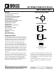

TMP35/TMP36/TMP37
Rev. F | Page 4 of 20
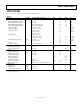
ABSOLUTE MAXIMUM RATINGS
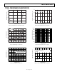
Table 2.
Parameter
1, 2
Rating
Supply Voltage 7 V
Shutdown Pin
GND ≤ SHUTDOWN
≤ +V
S
Output Pin GND ≤ V
OUT
≤ +V
S
Operating Temperature Range −55°C to +150°C
Die Junction Temperature 175°C
Storage Temperature Range −65°C to +160°C
IR Reflow Soldering
Peak Temperature 220°C (0°C/5°C)
Time at Peak Temperature Range 10 sec to 20 sec
Ramp-Up Rate 3°C/sec
Ramp-Down Rate −6°C/sec
Time 25°C to Peak Temperature 6 min
IR Reflow Soldering—Pb-Free Package
Peak Temperature 260°C (0°C)
Time at Peak Temperature Range 20 sec to 40 sec
Ramp-Up Rate 3°C/sec
Ramp-Down Rate −6°C/sec
Time 25°C to Peak Temperature 8 min
1
Digital inputs are protected; however, permanent damage can occur on
unprotected units from high energy electrostatic fields. Keep units in
conductive foam or packaging at all times until ready to use. Use proper
antistatic handling procedures.
2
Remove power before inserting or removing units from their sockets.
Stresses above those listed under Absolute Maximum Ratings
may cause permanent damage to the device. This is a stress
rating only; functional operation of the device at these or any
other conditions above those indicated in the operational
section of this specification is not implied. Exposure to absolute
maximum rating conditions for extended periods may affect
device reliability.
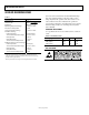
THERMAL RESISTANCE
θ
JA
is specified for the worst-case conditions, that is, a device in
socket.
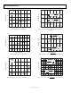
Table 3. Thermal Resistance
Package Type θ
JA
θ
JC
Unit
TO-92 (T-3) 162 120 °C/W
SOIC_N (R-8) 158 43 °C/W
SOT-23 (RJ-5) 300 180 °C/W
ESD CAUTION