
Data Sheet

October 2017 BNO080 Datasheet 1000-3927
www.hillcrestlabs.com © 2017 Hillcrest Laboratories, Inc. All rights reserved. 46 / 57
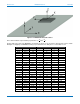
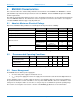
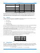
6.4 Electrical Characteristics
Parameter
Symbol
Conditions
Min
Typ
Max
Unit
Input high voltage
V
IH
V
DDIO
=1.7-2.7V
0.7*V
DDIO
V
DDIO
V
DDIO
=2.7-3.6V
0.55*V
DDIO
V
DDIO
Input low voltage
V
IL
V
DDIO
=1.7-2.7V
0.25*V
DDIO
V
DDIO
V
DDIO
=2.7-3.6V
0.3*V
DDIO
V
DDIO
Output high voltage
V
OH
V
DDIO
> 1.7V , I
OH
=10mA
0.8*V
DDIO
0.9*V
DDIO
V
DDIO
Output low voltage
V
OL
V
DDIO
> 3V, I
OL
=20mA
0.1*V
DDIO
0.2*V
DDIO
V
DDIO
POR Voltage threshold on
VDDIO-IN rising
V
DDIO_POT+
V
DDIO
falls at 1V/ms or
slower
1.45
V
POR Voltage threshold on
VDDIO-IN falling
V
DDIO_POT-
0.99
V
Figure 6-3: BNO080 electrical characteristics
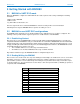
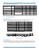
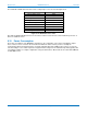
6.5 AC Characteristics
6.5.1 I
2
C Timing
The I
2
C interfaces of the BNO080 are compliant with the I
2
C specification [4]. The BNO080 provides master
functionality to the environmental sensors and slave functionality to the application processor
Parameter
Symbol
Conditions
Min
Max
Unit
SCL clock frequency
400
kHz
SCL high period
thigh
0.6
µs
SCL low period
tlow
1.3
µs
Rise time for SCL and SDA
10pF < Cb < 400pF
20+0.1Cb
ns
Fall time for SCL and SDA
10pF < Cb < 400pF
20 + 0.1Cb
ns
SDA setup time
tsu
0.1
µs
SDA hold time
th
0
µs
Hold time for start condition
thst
0.6
µs
Setup time for a stop condition
tsusp
0.6
µs
Idle time between accesses
tbf
1.3
µs
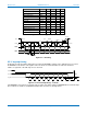
Figure 6-4: I
2
C timing parameters
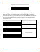
Figure 6-5: I
2
C timing
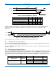
6.5.2 SPI timing
The Serial Peripheral Interface (SPI) is a synchronous serial interface. The BNO080 implements the slave side of
the interface for host communications. The BNO080 supports 4 wire mode and implements SPI mode 3: CPOL =
1 and CPHA = 1. SPI mode 3 implies that the clock idles at ‘1’ and that data is clocked in on the positive edge.
SDA
SCL
thst
tsu
th
tsusp
tbf
thigh
tlow