
Data Sheet

October 2017 BNO080 Datasheet 1000-3927
www.hillcrestlabs.com © 2017 Hillcrest Laboratories, Inc. All rights reserved. 18 / 57
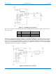
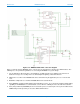
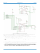
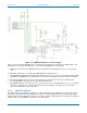
Figure 1-20: BNO080 SPI connection diagram
Figure 1-20 shows how the BNO080 can be connected to an external microcontroller via a SPI interface. The
following notes are provided as guidelines for connecting the BNO080 in a system design.
1. The H_INTN pin is the application interrupt line that indicates the BNO080 requires attention. This should be
tied to a GPIO with wake capability. The interrupt is active low.
2. NRST is the reset line for the BNO080 and can be either driven by the application processor or the board
reset.
3. BOOTN is sampled at reset. If low the BNO080 will enter bootloader mode.
4. Pin 4 (BOOTN) should be pulled high through a 10K Ohms resistor. To use the device firmware update (DFU)
capability of the BNO080, it is recommended to connect Pin 4 to a GPIO pin on the external microcontroller.
5. Pin 5 (PS1) and Pin 6 (PS0/WAKE) are the host interface protocol selection pins. Both pins must be high from
before reset until after the first assertion of H_INTN to select the SPI interface. Pin 5 may be tied to VDDIO.
Pin 6 must be connected to a GPIO so that the WAKE functionality can be performed.