
Data Sheet

October 2017 BNO080 Datasheet 1000-3927
www.hillcrestlabs.com © 2017 Hillcrest Laboratories, Inc. All rights reserved. 10 / 57
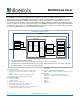
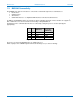
1.3.1 Pin Descriptions
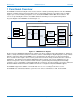
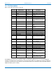
Figure 1-6 describes the function of each pin.
Pin
Number
BNO080 Name
Mode
Description
1
RESV_NC
NC
Reserved. No connect.
2
GND
Input
Ground
3
VDD
Input
Supply voltage (sensors) (2.4V
to 3.6V)
4
BOOTN
Input
Bootloader mode select
5
PS1
Input
Protocol Select pin 1
6
PS0/WAKE
Input
Protocol Select pin 0, also
used to wake processor in SPI
mode
7
RESV_NC
Input
Reserved. No connect.
8
RESV_NC
NC
Reserved. No connect.
9
CAP
External capacitor (100nF to
GND)
10
CLKSEL0
Input
Clock source selection. Internal
pulldown.
11
NRST
Input
Active low reset
12
RESV_NC
NC
Reserved. No connect.
13
RESV_NC
NC
Reserved. No connect.
14
H_INTN
Output
Interrupt to host device
15
ENV_SCL
Bidirectional
Environmental sensor I
2
C clock
16
ENV_SDA
Bidirectional
Environmental sensor I
2
C data
17
SA0/H_MOSI
Input
Lower address bit of device
address. In SPI mode, data
input
18
H_CSN
Input
SPI chip select, active low
19
H_SCL/SCK/RX
Bidirectional
Host Interface I
2
C clock, SPI
clock or UART RX
20
H_SDA/H_MISO/TX
Bidirectional
Host Interface I
2
C data, SPI
data out or UART TX
21
RESV_NC
NC
Reserved. No connect.
22
RESV_NC
NC
Reserved. No connect.
23
RESV_NC
NC
Reserved. No connect.
24
RESV_NC
NC
Reserved. No connect.
25
GND
Input
Ground
26
XOUT32/CLKSEL1
Output
32K crystal output / clock
source selection. Internal
pulldown.
27
XIN32
Input
32K crystal input. / external
clock
28
VDDIO
Input
Supply voltage (core and I/O
domain) (1.65V to 3.6V)
Figure 1-6: BNO080 pin descriptions
The BNO080 can operate from an internal oscillator, an external 32.768 kHz clock or an external 32.768 kHz
crystal. If an external clock is used it must be connected to pin 27. Hillcrest recommends a tolerance of 50ppm. If
a crystal is used it must be connected across pins 26 and 27. Hillcrest recommends using a crystal with tolerance
50ppm with 22pF capacitor loading.