
Data Sheet

Page 14 ams Datasheet
Document Feedback [v1-00] 2016-Nov-25
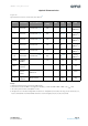
AS7263 − Detailed Description
Data Conversion Description
AS7263 spectral conversion is implemented via two photodi-
ode banks per device. Bank 1 consists of data from the S, T, U,
V photodiodes. Bank 2 consists of data from the R, T, U, W pho-
todiodes. Spectral conversion requires the integration time (IT
in ms) set to complete. If both photodiode banks are required
to complete the conversion, the 2nd bank requires an addition-
al IT ms. Minimum IT for a single bank conversion is 2.8 ms. If
data is required from all 6 photodiodes then the device must
perform 2 full conversions (2 x Integration Time).
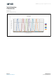
The spectral conversion process is controlled with BANK Mode
settings as follows:
BANK Mode 0: Data will be available in registers S, T, U & V (R
and W registers will be zero)
BANK Mode 1: Data will be available in registers R, T, U & W (V
and W registers will be zero)
BANK Mode 2: Data will be available in registers R, S, T, U, V & W
When the bank setting is Mode 0, Mode 1, or Mode 2, the spec-
tral data conversion process operates continuously, with new
data available after each IT ms period. In the continuous modes,
care should be taken to assure prompt interrupt servicing so
that integration values from both banks are all derived from the
same spectral conversion cycle.
BANK Mode 3: Data will be available in registers R, S, T, U, V & W
in One-Shot mode
When the bank setting is Mode 3, the device operates in
One-Shot mode. Spectral conversion occurs only when bit 0 of
the control register (1SHOT) is set to 1. The 1SHOT bit in the
control register is subsequently cleared by hardware at the
same time the DATA_RDY bit is set to 1 indicating the availability
of spectral conversion result data. The One-Shot mode is in-
tended for use when it is critical to ensure that spectral conver-
sion results are obtained contemporaneously.