
Data Sheet

Page 36 ams Datasheet
Document Feedback [v1-01] 2017-Mar-17
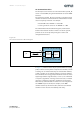
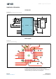
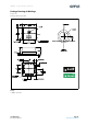
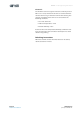
AS7262 − PCB Pad Layout
Suggested PCB pad layout guidelines for the LGA device are
shown.
Figure 35:
Recommended PCB Pad Layout
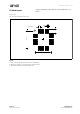
Note(s):
1. Unless otherwise specified, all dimensions are in millimeters.
2. Dimensional tolerances are ±0.05mm unless otherwise noted.
3. This drawing is subject to change without notice.
PCB Pad Layout
1
4.40
0.30
0.65
1.10
4.60
Unit: mm