
Data Sheet

[AK9753]
017005237-E-00 2017/04
- 26 -
12.1.5. WRITE Command
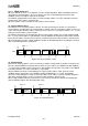
When the R/w bit set to “0”, the AK9753 executes a WRITE Operation. The AK9753 will out an
Acknowledge signal and receive the second byte, after receiving a Start condition and first one byte
(Slave address) in a WRITE Operation. The second byte has an MSB-first configuration, and specifies
the address of the internal control register.
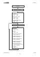
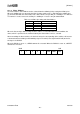
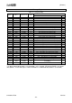
MSB LSB
A7
A6
A5
A4
A3
A2
A1
A0
Figure 12.5. Register Address
The AK9753 will generate an Acknowledge and receive the third byte after receiving the second byte
(Register Address).
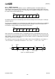
The data after the third byte is the control data. The control data consists of 8-bit and has an MSB-first
configuration. The AK9753 generates an Acknowledge for each byte received. The data transfer is
terminated by a Stop condition, generated by the master device.
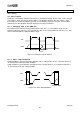
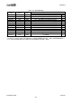
MSB LSB
D7
D6
D5
D4
D3
D2
D1
D0
Figure 12.6. Control data
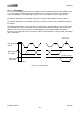
Two or more bytes can be written at once. The AK9753 generates an Acknowledge and receives the
next data after receiving the third byte (Control Data). When the following data is transmitted without a
Stop condition, after transmitting one byte, the internal address counter is automatically incremented,
and data is written in the next address.
The automatic increment function works in the address from 11H to 1CH.Wthen the start address is
“11H”, the address is repeatedly incremented as. “11H -> 12H ->…..-> 1CH -> 11H -> 12H…”
SDA
S
Slave
Address
R/W= 0
ACK
Register
Address(n)
ACK
DATA(n)
DATA(n+1)
DATA(n+x)
P
Start
Stop
ACK
ACK
ACK
ACK
Figure 12.7. WRITE Operation