[AK9753] AK9753 IR Sensor IC with I2C I/F 1. General Description The AK9753 is a low power and compact infrared-ray (IR) sensor module. It is composed of four quantum IR sensors and an integrated circuit (IC) for characteristic compensation. The four IR sensors’ offset and gain variations are calibrated at shipment. An integral analog-to-digital converter provides 16-bits data outputs. The AK9753 is suitable for several feet human detector by using external lens. 2.
[AK9753] 3. Table of Contents 1. 2. 3. 4. General Description ............................................................................................................................ 1 Features .............................................................................................................................................. 1 Table of Contents ................................................................................................................................
[AK9753] 17. Data Sampling Period ................................................................................................................... 41 18. Spectrum Sensitivity (Reference).................................................................................................. 42 19. Field of View (Reference) .............................................................................................................. 43 20. Recommended External Circuits............................................
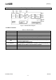
[AK9753] 4. Block Diagram and Functions 4.1. Block Diagram Figure 4.1 AK9753 Block Diagram 4.2. Block Functions Table 4.1. Block Functions Block 4 x IR MUX TIA AMP Temperature Sensor ADC I2C Interface EEPROM OSC POR Function Four IR Sensor Matrix Switch Photocurrents of IR Sensor are converted to voltage signals. Programmable gain amplifier to adjust the outputs. Built-in Temperature Sensor The amplifier output and the built-in temperature sensor output are converted to digital signals.
[AK9753] 5. Pin Configurations and Functions 5.1. Pin Configurations VDD 1 10 VSS CAD0 2 9 TEST CAD1 3 8 DVDD INT 4 7 SCL PDN 5 6 SDA Top View Figure 5.1 Pin Configurations 5.2. Pin Functions Table 5.1 Pin Functions Pin No. 1 Name I/O VDD - 2 CAD0 I 3 CAD1 I 4 INT O 5 PDN I 6 SDA I/O 7 SCL I 8 9 10 DVDD TEST VSS I - Function Analog Power Supply Pin Slave address 0. CAD0 pin should be connected to VDD or VSS.
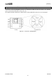
[AK9753] 6. IR Sensors Configuration / Observable Area 6.1. IR Sensor’s Configurations The four IR sensors which AK9753 includes are arranged as shown in Figure 6.1 IR1(2, 3, 4) is defined as the measurement data of IR sensor 1(2, 3, 4). The upper (left, lower, right) side is defined as the side on which IR sensor 1(2, 3, 4) is arranged. Figure 6.1.
[AK9753] 7. Absolute Maximum Ratings (VSS= 0V) Parameter Power Supply Input Current Input Voltage (* 1) VDD pin, DVDD pin All pins CAD0 pin, CAD1 pin, INT pin, PDN pin, TEST pin, SCL pin, SDA pin Symbol V+ Iin Min. -0.6 -10 Max. 4.6 10 Unit V mA Vin -0.6 4.6 V Tst -30 85 ºC Storage Temperature Note: * 1. Vin should be always lower than (V+) + (0.6V). WARNING: Operation at or beyond these limits may result in permanent damage to the device.
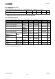
[AK9753] 9. Power Supply Conditions (Unless otherwise specified, VDD=1.71 ~ 3.63V, DVDD= 1.65V ~ VDD, Ta= -30 ~ 85ºC) Parameter Symbol Min. Typ. Power Supply Rise Time (* 4, * 5) Power-on Reset Time (* 4, * 5) Shutdown Voltage (* 5, * 6) Power Supply Interval Time (* 4, * 5, * 6) Time until VDD, DVDD, and PDN are set to the operating voltage from 0.2V. Time until AK9753 becomes Power down Mode after PSUP. Shutdown Voltage for POR re-starting. Voltage retention time below SDV1 for POR re-starting. Max.
[AK9753] 10. Electrical Characteristics・Optical Charateristics 10.1. Analog Characteristics (Unless otherwise specified, VDD= 1.71 ~ 3.63V, DVDD= 1.65V ~ VDD, Ta= -30 ~ 85ºC) The following are the characteristics of sensor without lens. Parameter IR output resolution IR offset code IR output code Symbol All output currents of four IR sensors are Zero. ・Reference data only, not tested. ・Ttgt= 35ºC, Ta= 25ºC ±3ºC ・2’s complement Min. Typ. 16 Max.
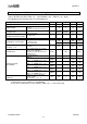
[AK9753] 10.2. Digital Characteristics 10.2.1. EEPROM (Unless otherwise specified, VDD= 1.71 ~ 3.63V, DVDD= 1.65V ~ VDD, Ta= -30 ~ 85ºC) Parameter Symbol Min. Typ. Max. Retention Time @Ta= 85ºC Ehold 10 Endurance 1000 Note: * 8. VDD (EVDD) should be greater than 3.0V, when writing EEPROM. Unit years times 10.2.2. DC Characteristics (Unless otherwise specified, VDD= 1.71 ~ 3.63V, DVDD= 1.65V ~ VDD, Ta= -30 ~ 85ºC) Parameter Symbol Min. Typ. Max.
[AK9753] 10.2.3. AC Characteristics (1): Standard Mode (100 kHz) (Unless otherwise specified, VDD= 1.71 ~ 3.63V, DVDD= 1.65V ~ VDD, Ta= -30 ~ 85ºC) Parameter Symbol Min. Typ. Max. SCL frequency fSCL 100 SDA bus idle time to the next fBUF 4.7 command input Start condition Hold time tHD:STA 4.0 Clock Low period tLOW 4.7 Clock High period tHIGH 4.0 Start condition set-up time tSU:STA 4.7 Data hold time tHD:DAT 0 Data set-up time tSU:DAT 250 Rise time SDA pin, tR 1.
[AK9753] tHIGH tF tR tLOW SCL tSU:STA tHD:DAT tHD:STA tSU:DAT tSU:STO SDAIN tDH tBUF SDA OUT Figure 10.1. Bus Timing SCL SDA 8th bit STOP ACK WORDn START tWR ≧ 10ms Figure 10.2.
[AK9753] 11. Functional Descriptions 11.1 Power Supply States When VDD, DVDD and PDN turn on from the state of VDD= DVDD= OFF(0V), Power-on Reset(POR) automatically operates, all registers will be initialized, and the AK9753 will be set to Stand-by Mode. Although all states of the Following table can exist, the state 2 is prohibited. State 1 2 3 4 5 VDD pin OFF(0V) OFF(0V) 1.71 ~ 3.63V 1.71 ~ 3.63V 1.71 ~ 3.63V 6 1.71 ~ 3.63V Table 11.1.
[AK9753] 11.3 Operating Mode 11.3.1. Normal Mode/Switch Mode AK9753 has two Modes, Normal Mode and Switch Mode. Normal Mode is the mode which controls AK9753 by using I2C interface. The digital output the four IR sensors and the internal temperature sensor can be used through the I2C interface in Normal Mode. INT output also can be used. Switch Mode is the mode which uses only INT output without using I2C interface.
[AK9753] 11.3.2. Normal Mode There are the eight Modes in Normal Mode. (1) Power down Mode (2) Stand-by Mode (3) Single shot Mode (4) Continuous Mode 0 (5) Continuous Mode 1 (6) Continuous Mode 2 (7) Continuous Mode 3 (8) EEPROM access Mode Power down Mode: The all circuits are powered down for saving the current consumption.
[AK9753] On initial power-on with PDN pin= “H”, AK9753 is in Stand-by Mode. Based on EMODE [2:0] setup, the AK9753 shifts to the selected Mode, and starts operating. Any Mode changing should be done via Stand-by Mode. 11.3.3. Switch Mode There are two Modes in Switch Mode. (1) Power down Mode (2) Measurement Mode Power down Mode: The all Circuits are powered down for decreasing the current consumption.
[AK9753] 11.4 Descriptions for each Operating Mode 11.4.1. Power down Mode (PDN pin= “L”) All circuits are powered off and all internal resisters are reset with PDN pin= “L”. The all functions of AK9753 do not work in this Mode. 11.4.2. Stand-by Mode (EMODE [2:0] = “000”) All circuits are powered off except for POR circuit. All registers can be accessed in this Mode. Read / Write register data are retained, and reset by software reset. However, EEPROM data cannot be read / written in this Mode.
[AK9753] 11.4.5. Continuous Mode 0 (EMODE [2:0] = “100”) When Continuous Mode 0 (EMODE [2:0] = “100”) is selected the measurement is automatically repeated at the cycle which is determined by the digital filter cut-off frequency (EFC [2:0], Table 16.2). When a measurement have been done, the measurement data is stored to the measurement register (IR1L to TMPH), and new measurement is started. * Please refer to Table16.1 for first measurement time.
[AK9753] 11.5 Read Measurement Data When a measurement data is stored to the measurement register, DRDY bit of ST1 register changes to “1”. This state is called “Data Ready”. It can be set up so that INT output “H”, when the DRDY bit is “1”, by setting up the interruption register. The read-out procedure is detailed here. (Single shot Mode is used as an example.) The same procedure can also be applied the Continuous Mode 0 (1, 2, and 3). 11.5.1.
[AK9753] 11.5.2. Read-out Data within a measurement Period The measurement data register is retained within a measurement period, so the data can be read out within the measurement period. When data is read out within the measurement period, the previous data retained is read out. (N-1) PD (N) Measurement (N+1) Measurement PD Internal Buffer data(N-1) data(N) Measurement data register data(N-1) PD data(N+1) data(N) data(N) DRDY Read-out data ST1 data(N) ST2 ST1 data(N) ST2 Figure 11.7.
[AK9753] When a data read begins after the end of the Nth measurement, and when data read cannot be completed until the end of the (N+1)th measurement, the measurement data registers are protected to read data normally. In this case, because the(N+1)th data has been skipped, the DOR bit transitions to “1”.
[AK9753] Power On Wait Time 3.
[AK9753] 12. Serial Interface The I C bus interface of the AK9753 supports Standard Mode (Max. 100kHz) and High Speed Mode (Max. 400kHz). 2 12.1. Data Transfer Initially the start condition should be input to access the AK9753 through the bus. Next, send a one byte slave address, which includes the device address. The AK9753 compares the slave address, and if these addresses match, the AK9753 generates an acknowledge signal and executes a Read / Write command.
[AK9753] 12.1.3. Acknowledge The device transmitting data will release the SDA line after transmitting one byte of data (SDA line state is “H”). The device receiving data will pull the SDA line to “L” during the next clock. This operation is called “Acknowledge”. The Acknowledge signal can be used to indicate successful data transfers. The AK9753 will output an acknowledge signal after receiving a Start condition and Slave address.
[AK9753] 12.1.4. Slave Address The Slave address of the AK9753 can be selected from the following list by setting the CAD0/1 pins. When the CAD0/1 pins are connected to VSS, the Slave address bit is = 64H. When the CAD0/1 pins are connected to VDD, the Slave address bit is 65H. Do not set up “CAD1 pin = CAD0 pin = H” while the I2C interface is used, because the “CAD1 pin = CAD0 pin = H state is only for Switch Mode. Table 12.1.
[AK9753] 12.1.5. WRITE Command When the R/w bit set to “0”, the AK9753 executes a WRITE Operation. The AK9753 will out an Acknowledge signal and receive the second byte, after receiving a Start condition and first one byte (Slave address) in a WRITE Operation. The second byte has an MSB-first configuration, and specifies the address of the internal control register. MSB A7 LSB A6 A5 A4 A3 A2 A1 A0 Figure 12.5.
[AK9753] 12.1.6. READ Command When the R/W bit is set to “1”, the AK9753 executes a READ Operation. When the AK9753 transmits data from the specified address, the master device generates an Acknowledge instead of a Stop condition and the next address data can be read out. The AK9753 supports both current address read and random address read. The automatic increment function works in the address of 05H to 10H. When the address 10H is read out, the next address returns to 05H.
[AK9753] 12.1.7. EEPROM Write Timing Writing data to EEPROM should be done at shown timing as the following. SCL 8th bit ACK STOP WORD n tWR ≥ 10ms Stop DATA P tWR ≥ 10ms Stop P ACK Data S ACK ACK ACK ACK ACK ACK ACK Start R/W= “0” EEPROM Address EKEY Register Address Slave P S Address DATA ACK Start EMODE Register Address Slave S Address R/W= “0” Stop Start R/W= “0” Slave SDA S Address START Start SDA Figure 12.10.
[AK9753] 13. Memory Map Table 13.1.
[AK9753] Table 13.2.
[AK9753] 14. Registers Functional Descriptions Table 14.1.
[AK9753] 3). INFO1: Information (Read Only Registers) Address Name D7 D6 D5 02H INFO1 0 0 0 D4 0 D3 0 D2 0 D1 0 D0 1 D4 0 D3 0 D2 0 D1 0 D0 0 D4 IR13H 0 D3 IR13L 0 D2 IR24H 0 D1 IR24L 0 D0 DR 0 INFO1 [7:0]: Information for AKM use only. 4). INFO2: Information (Read Only Registers) Address Name D7 D6 D5 03H INFO2 0 0 0 INFO2 [7:0]: Reserve 5).
[AK9753] 6). ST1: Status 1 (Read Only Registers) Address Name D7 D6 05H ST1 Reset 1 1 D5 D4 D3 D2 1 1 1 1 D1 DOR 0 D0 DRDY 0 DRDY: Data Ready “0”: Normal State “1”: Data Ready The DRDY bit turns to “1”, when the data is ready to be read. This bit turns back to “0”, when either the ST2 register or one of the measured data (IRS1L to TMPH) is read. DOR: Data Overrun “0”: Normal State “1”: Data Overrun The DOR bit turns to “1”, when the data reading is skipped.
[AK9753] 7). IRxL, IRxH: Measurement Data of IR sensor (x= 1, 2, 3, 4) (Read Only Registers) Address Name D7 D6 D5 D4 D3 D2 D1 IRxL_7 IRxL_6 IRxL_5 IRxL_4 IRxL_3 IRxL_2 IRxL_1 06,08,0A,0C H IRxL 07,09,0B,0D H IRxH IRxH_15 IRxH_14 IRxH_13 IRxH_12 IRxH_11 IRxH_10 IRxH_9 Reset 0 0 0 0 0 0 0 D0 IRxL_0 IRxH_8 0 Measurement Data of IR sensor IRxL [7:0]: Least significant 8-bits in output data IRxH [15:8]: Most significant 8-bits in output data 16-bit data is stored in tow’s compliment format. Table 14.2.
[AK9753] 8). TMPL, TMPH: Measurement Data of the Integrated temperature Sensor (Read / Write Registers) Address Name D7 D6 D5 D4 D3 D2 D1 D0 TMPL_7 TMPL_6 TMPL_5 TMPL_4 TMPL_3 TMPL_2 TMPL_1 TMPL_0 0EH TMPL TMPH_8 0FH TMPH TMPH_15 TMPH_14 TMPH_13 TMPH_12 TMPH_11 TMPH_10 TMPH_9 Reset 0 0 0 0 0 0 0 0 Note: * 15. TMPL_0 bit to TMPL_5 bit are fixed to “0”.
[AK9753] 10).
[AK9753] 11). EHYS13, EHYS24: Hysteresis setting of Threshold Level / Polarity setting of INT output. (Read / Write Registers) Address Name D7 D6 D5 D4 D3 D2 D1 D0 EHYS13_4 EHYS13_3 EHYS13_2 EHYS13_1 EHYS13_0 19H EHYS13 EHYS24_4 EHYS24_3 EHYS24_2 EHYS24_1 EHYS24_0 1AH EHYS24 Reset 1 1 1 0 0 0 0 0 Hysteresis setting for Threshold levels ETHYS13, EHYS24: Hysteresis setting for threshold levels 5-bit This register is used only in Switch Mode (ECOPY). Table 14.6.
[AK9753] 12). EINTEN: Interrupt Source setting (Read / Write Registers) Address Name D7 D6 D5 D4 D3 1BH EINTEN IR13HI IR13LI Reset 1 1 0 0 0 D2 IR24HI 0 D1 IR24LI 0 D0 DRI 0 The interrupt to the HOST MCU via the INT output can be obtained by the following methods: INT output turns to “Active”, when at least one of the enabled interrupt source conditions is satisfied. HOST MCU can identify the interrupt source by reading the Interrupt Source Status (INST).
[AK9753] 13).
[AK9753] 15. EEPROM Functional Descriptions Table 15.1.
[AK9753] 16. First data Determination Time The First data determination time is defined as the time between “setting the registers” and “determining the measurement data”. It depends on Measurement Mode setting and Digital Filter setting. Since the first data determination time also depends on the OCS frequency, Min./Max. is Typ. ±10%. Table 16.1.
[AK9753] 18. Spectrum Sensitivity (Reference) Figure 18.1.
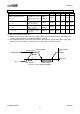
[AK9753] 19. Field of View (Reference) Parameter Symbol Min. Typ. Max. Unit Field of View (* 19) FOV deg(º) ±80 Note: * 19. The combined range observed by Upper/Lower (Left/Right) sensors. Reference data only, not tested. 1.2 IR1 (or IR2) R1(R2) Standardized IR Output 1 IR3 (or IR4) R3(R4) 0.8 0.6 0.4 0.2 0 -100 -50 0 50 Angle θ[°] 100 Figure 19.1. Field of View (Typ.) Ambient Temperature: Ta=25℃ Block Body: Φ12.
[AK9753] 20. Recommended External Circuits DVDD DVDD DVDD DVDD DVDD VDD1 330Ω Power for I/F SCL DVDD 1.0µF VDD 1.0µF VSS I2C I/F SDA AKM INT AK9753 CAD0 TEST CAD1 INT INPUT Slave Address Select: CAD0 and CAD1 must be connected to VDD or VSS. Digital Output GND PDN VSS HOST MCU VSS VSS VSS Figure 20.1.
[AK9753] 21. Package 21.1.Outline Dimensions 10-pin SON (Unit mm) Unless otherwise specified: ±0.
[AK9753] 21.2.
[AK9753] 21.3.
[AK9753] 22. Structure of Filter Block and IR Sensors (Reference) Structure of Filter Block and IR Sensors is as shown Figure 22.1. Structure of Filter Block is as shown Figure 22.2. Structure of IR Sensors is as shown Figure 22.3. To consider structure and the FOV properties of AK9753 is needed for designing the external lens. 1100um 700um Figure 22.1. Structure of Filter Block and IR Sensors (Cross section) Figure 22.2. Structure of Filter Block (Overhead view) Figure 22.3.
[AK9753] 23. Ordering Guide AK9753AE -30 ~ 85ºC 10-pin SON 24.
[AK9753] IMPORTANT NOTICE 0. Asahi Kasei Microdevices Corporation (“AKM”) reserves the right to make changes to the information contained in this document without notice. When you consider any use or application of AKM product stipulated in this document (“Product”), please make inquiries the sales office of AKM or authorized distributors as to current status of the Products. 1. All information included in this document are provided only to illustrate the operation and application examples of AKM Products.