
Data Sheet

Page 29
RFM95/96/97/98(W)
Tel: + 86-755-82973805 Fax: +86- 755-82973550 E-mail: sales@hoperf.com http:/ / www.hoperf.com
WIRELESS & SENSING PRELIMINARY DATASHEET
4.1.2. LoRa
TM
Digital Interface
The LoRa
TM
modem comprises three types of digital interface, static configuration registers, status registers and a FIFO
data buffer. All are accessed through the RFM95/96/97/98(W)’s SPI interface - full details of each type of register are
given below. Full listings of the register addresses used for SPI access are given in Section 6.4.
4.1.2.1. LoRa
TM
Configuration Registers
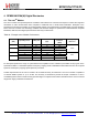
Configuration registers are accessed through the SPI interface. Registers are readable in all device mode including Sleep.
However, they should be written only in Sleep and Stand-by modes. Please note that the automatic top level
sequencer (TLS modes) are not available in LoRa
TM
mode and the configuration register mapping changes as
shown in Table 85. The content of the LoRa
TM
configuration registers is retained in FSK/OOK mode. For the functionality of
mode registers common to both FSK/OOK and LoRa
TM
mode, please consult the Analog and RF Front End section of this
document (Section 5).
4.1.2.2. Status Registers
Status registers provide status information during receiver operation.
4.1.2.3. LoRa
TM
Mode FIFO Data Buffer
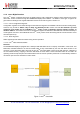
Overview
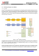
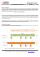
The RFM95/96/97/98(W) is equipped with a 256 byte RAM data buffer which is uniquely accessible in LoRa mode. This
RAM area, thereafter reffered to as the FIFO Data buffer, is fully customizable by the user and allows access to the
received, or to be transmitted, data. All access to the LoRa
TM
FIFO data buffer is done via the SPI interface. A diagram of
the user defined memory mapping of the FIFO data buffer is shown below. These FIFO data buffer can be read in all
operating modes except sleep and store data related to the last receive operation performed. It is automatically cleared of
old content upon each new transition to receive mode.
Figure 7.
LoRa
TM
data buffer