
Data Sheet


Page 15
RFM95/96/97/98(W)
Tel: + 86-755-82973805 Fax: + 86- 755-82973550 E-mail: sales@hoperf.com http:/ / www.hoperf.com
WIRELESS & SENSING PRELIMINARY DATASHEET
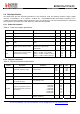
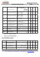
ACR
Adjacent Channel Rejection
FDA = 5 kHz, BR=4.8kb/s
Offset = +/- 25 kHz or +/- 50kHz
169MHz Band
434 MHz Band
8-900 MHz Band
-
-
-
59
56
50
-
-
-
dB
dB
dB
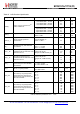
BI_HF
Blocking Immunity, higher bands
Offset = +/- 1 MHz
Offset = +/- 2 MHz
Offset = +/- 10 MHz
-
-
-
71
76
84
-
-
-
dB
dB
dB
BI_LF
Blocking Immunity, lower bands
Offset = +/- 1 MHz
Offset = +/- 2 MHz
Offset = +/- 10 MHz
-
-
-
71
72
78
-
-
-
dB
dB
dB
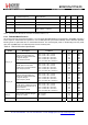
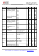
IIP2
2nd order Input Intercept Point
Unwanted tones are 20 MHz
above the LO
Highest LNA gain
-
+55
-
dBm
IIP3_HF
3rd order Input Intercept point
Unwanted tones are 1MHz and
1.995 MHz above the LO
Higher bands
Highest LNA gain G1
LNA gain G2, 4dB sensitivity hit
-
-
-12.5
-8.5
-
-
dBm
dBm
IIP3_LF
3rd order Input Intercept point
Unwanted tones are 1MHz and
1.995 MHz above the LO
Lower bands
Highest LNA gain G1
LNA gain G2, 2.5dB sensitivity hit
-
-
-22
-16
-
-
dBm
dBm
BW_SSB Single Side channel filter BW Programmable 2.7 - 250 kHz
IMR
Image Rejection
Wanted signal 3dB over sensitivity
BER=0.1%
-
48
-
dB
IMA Image Attenuation
- 57 - dB
DR_RSSI
RSSI Dynamic Range
AGC enabled Min
Max
-
-
-127
0
-
-
dBm
dBm
* RxBw = 83 kHz (Single Side Bandwidth)
** RxBw = 50 kHz (Single Side Bandwidth)
*** RxBw = 250 kHz (Single Side Bandwidth)
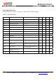
2.4.4. FSK/OOK Mode Transmitter
Table 54 Transmitter Specification
Symbol
Description
Conditions
Min
Typ
Max
Unit
RF_OP
RF output power in 50 ohms
on RFO pin (High efficiency PA).
Programmable with steps
Max
Min
+11
-
+14
-1
-
-
dBm
dBm
ΔRF_
OP_V
RF output power stability on RFO
pin versus voltage supply.
VDD = 2.5 V to 3.3 V
VDD = 1.8 V to 3.7 V
-
-
3
8
-
-
dB
dB
RF_OPH
RF output power in 50 ohms, on
PA_BOOST pin (Regulated PA).
Programmable with 1dB steps Max
Min
-
-
+17
+2
-
-
dBm
dBm