
Data Sheet

Page 108
RFM95/96/97/98(W)
Tel: + 86-755-82973805 Fax: + 86- 755-82973550 E-mail: sales@hoperf.com http:/ / www.hoperf.com
WIRELESS & SENSING PRELIMINARY DATASHEET
7. Application Information
7.1. Crystal Resonator Specification
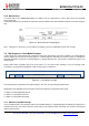
Table 89 shows the crystal resonator specification for the crystal reference oscillator circuit of the RFM95/96/97/98(W).
This specification covers the full range of operation of the RFM95/96/97/98(W) and is employed in the reference design.
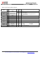
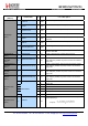
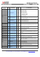
Table 89 Crystal Specification
Symbol
Description
Conditions
Min
Typ
Max
Unit
FXOSC XTAL Frequency
- 32 - MHz
RS XTAL Serial Resistance
- 30 TBC ohms
C0 XTAL Shunt Capacitance
- 2.8 TBC pF
CFOOT External Foot Capacitance On each pin XTA and XTB 8 15 22 pF
CLOAD Crystal Load Capacitance
6 - 12 pF
Notes - the initial frequency tolerance, temperature stability and ageing performance should be chosen in accordance
with the target operating temperature range and the receiver bandwidth selected.
- the loading capacitance should be applied externally, and adapted to the actual Cload specification of the XTAL.
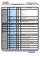
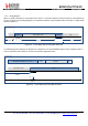
7.2. Reset of the Chip
A power-on reset of the RFM95/96/97/98(W) is triggered at power up. Additionally, a manual reset can be issued by
controlling pin 6.
7.2.1. POR
If the application requires the disconnection of VDD from the RFM95/96/97/98(W), despite of the extremely low Sleep
Mode current, the user should wait for 10 ms from of the end of the POR cycle before commencing communications over
the SPI bus. Pin 7 (NRESET) should be left floating during the POR sequence.
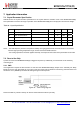
Figure 42. POR Timing
Diagram
Please note that any CLKOUT activity can also be used to detect that the chip is ready.