RFM95/96/97/98(W) RFM95/96/97/98(W) - Low Power Long Range Transceiver Module V1.0 GENERAL DESCRIPTION The RFM95/96/97/98(W) transceivers feature the LoRaTM long range modem that provides ultra-long range spread spectrum communication and high interference immunity whilst minimising current consumption. Using Hope RF’s patented LoRaTM modulation technique RFM95/96/97/98(W) can achieve a sensitivity of over 148dBm using a low cost crystal and bill of materials.
RFM95/96/97/98(W) Section 1. 2. Page General Description ................................................................................................................................................. 9 1.1. Simplified Block Diagram ................................................................................................................................. 9 1.2. Product Versions .....................................................................................................................
RFM95/96/97/98(W) Section Page 4.2.13. Packet Mode ........................................................................................................................................... 66 4.2.14. io-homecontrol® Compatibility Mode ...................................................................................................... 74 4.3. 5. SPI Interface ................................................................................................................................................
RFM95/96/97/98(W) Section Page 7.4.2. Sequencer Configuration......................................................................................................................... 115 8. 7.5. Example CRC Calculation ........................................................................................................................117 7.6. Example Temperature Reading ................................................................................................................
RFM95/96/97/98(W) Section Page Table 1. RFM95/96/97/98(W) Device Variants and Key Parameters .............................................................................10 Table 2. Absolute Maximum Ratings .............................................................................................................................12 Table 3. Operating Range .............................................................................................................................................
RFM95/96/97/98(W) Section Page Table 40. High Frequency Additional Registers ..........................................................................................................101 Table 41. Table 42. Table 43. Table 44. Table 45. Table 46. Table 47. Crystal Specification ....................................................................................................................................108 Listen Mode with PreambleDetect Condition Settings ...........................................
RFM95/96/97/98(W) Section Page Figure 1. Block Diagram ...............................................................................................................................................9 Figure 2. Pin Diagrams ...............................................................................................................................................10 Figure 3. RFM95/96/97/98(W) Block Schematic Diagram .........................................................................................
RFM95/96/97/98(W) Section Page Figure 40. Listen Mode with No Preamble Received .................................................................................................110 Figure 41. Figure 42. Figure 43. Figure 44. Figure 45. Figure 46. Figure 47. Figure 48. Figure 49. Figure 50. Figure 51. Figure 52. Listen Mode with Preamble Received .......................................................................................................110 Wake On PreambleDetect State Machine .................
RFM95/96/97/98(W) WIRELESS & SENSING PRELIMINARY DATASHEET 1. General Description The RFM95/96/97/98(W) incorporates the LoRaTM spread spectrum modem which is capable of achieving significantly longer range than existing systems based on FSK or OOK modulation. With this new modulation scheme sensitivities 8 dB better than FSK can be achieved with a low-cost, low-tolerance, crystal reference.
RFM95/96/97/98(W) WIRELESS & SENSING PRELIMINARY DATASHEET 1.2. Product Versions The features of the three product variants are detailed in the following table. Table 48 RFM95/96/97/98(W) Device Variants and Key Parameters Part Number Frequency Range Spreading Factor Bandwidth Effective Bitrate Est. Sensitivity RFM95W 868/915 MHz 6 - 12 7.8 - 500 kHz .018 - 37.5 kbps -111 to -148 dBm RFM97W 868/915 MHz 6-9 7.8 - 500 kHz 0.11 - 37.5 kbps -111 to -139 dBm 433/470MHz 6- 12 7.
RFM95/96/97/98(W) WIRELESS & SENSING PRELIMINARY DATASHEET 1.4. Pin Description Number Name Type Description Description Stand Alone Mode 1 GND - Ground 2 MISO I SPI Data output 3 MOSI O SPI Data input 4 SCK I SPI Clock input 5 NSS I SPI Chip select input 6 RESET I/O Reset trigger input 7 DIO5 I/O Digital I/O, software configured 8 GND - Ground 9 ANT - RF signal output/input.
RFM95/96/97/98(W) WIRELESS & SENSING PRELIMINARY DATASHEET 2. Electrical Characteristics 2.1. ESD Notice The RFM95/96/97/98(W) is a high performance radio frequency device. It satisfies: Class 2 of the JEDEC standard JESD22-A114-B (Human Body Model) on all pins. Class III of the JEDEC standard JESD22-C101C (Charged Device Model) on all pins It should thus be handled with all the necessary ESD precautions to avoid any permanent damage. 2.2.
RFM95/96/97/98(W) WIRELESS & SENSING PRELIMINARY DATASHEET 2.4. Chip Specification The tables below give the electrical specifications of the transceiver under the following conditions: Supply voltage VDD=3.3 V, temperature = 25 °C, FXOSC = 32 MHz, FRF = 169/434/868/915 MHz (see specific indication), Pout = +13dBm, 2-level FSK modulation without pre-filtering, FDA = 5 kHz, Bit Rate = 4.8 kb/s and terminated in a matched 50 Ohm impedance, shared Rx and Tx path matching., unless otherwise specified. 2.4.
RFM95/96/97/98(W) WIRELESS & SENSING PRELIMINARY FRC RC Oscillator frequency After calibration BRF Bit rate, FSK BRO DATASHEET - 62.5 - kHz Programmable values (1) 1.2 - 300 kbps Bit rate, OOK Programmable 1.2 - 32.768 kbps BRA Bit Rate Accuracy ABS(wanted BR - available BR) - - 250 ppm FDA Frequency deviation, FSK (1) Programmable FDA + BRF/2 =< 250 kHz 0.6 - 200 kHz Note For Maximum Bit rate the maximum modulation index is 0.5. 2.4.3.
RFM95/96/97/98(W) WIRELESS & SENSING PRELIMINARY DATASHEET ACR Adjacent Channel Rejection FDA = 5 kHz, BR=4.
RFM95/96/97/98(W) RF_OPH_ MAX Max RF output power, on PA_BOOST pin ΔRF_ RF output power stability on PA_BOOST pin versus voltage supply. OPH_V ΔRF_T RF output power stability versus temperature on PA_BOOST pin.
RFM95/96/97/98(W) WIRELESS & SENSING PRELIMINARY DATASHEET Table 55 LoRa Receiver Specification. Symbol Description Conditions Supply current in receiver LoraTM mode, LnaBoost off IDDR_L Supply current in transmitter mode IDDT_L IDDT_H_L Supply current in transmitter mode with an external impedance transformation Min. Typ Max Unit Lower Bands, Lower BW Lower Bands, BW = 125 kHz Lower Bands, BW = 250 kHz Lower Bands, BW = 500 kHz - TBC 11.5 12.4 13.
RFM95/96/97/98(W) WIRELESS & SENSING Symbol PRELIMINARY Min.
RFM95/96/97/98(W) WIRELESS & SENSING PRELIMINARY DATASHEET 2.4.6. Digital Specification Conditions: Temp = 25° C, VDD = 3.3 V, FXOSC = 32 MHz, unless otherwise specified. Table 57 Digital Specification Symbol Description Conditions Min Typ Max Unit VIH Digital input level high 0.8 - - VDD VIL Digital input level low - - 0.2 VDD VOH Digital output level high Imax = 1 mA 0.9 - - VDD VOL Digital output level low Imax = -1 mA - - 0.
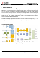
RFM95/96/97/98(W) 3. RFM95/96/97/98(W) Features This section gives a high-level overview of the functionality of the RFM95/96/97/98(W) low-power, highly integrated transceiver. The following figure shows a simplified block diagram of the RFM95/96/97/98(W). Figure 3. RFM95/96/97/98(W) Block Schematic Diagram RFM95/96/97/98(W) is a half-duplex, low-IF transceiver. Here the received RF signal is first amplified by the LNA. The LNA inputs are single ended to minimise the external BoM and for ease of design.
RFM95/96/97/98(W) All major parameters of the RF front end and digital state machine are fully configurable via an SPI interface which gives access to RFM95/96/97/98(W)’s configuration registers. This includes a mode auto sequencer that oversees the transition and calibration of the RFM95/96/97/98(W) between intermediate modes of operation in the fastest time possible. The RFM95/96/97/98(W) are equipped with both standard FSK and long range spread spectrum (LoRaTM) modems.
RFM95/96/97/98(W) WIRELESS & SENSING PRELIMINARY DATASHEET 4. RFM95/96/97/98(W) Digital Electronics 4.1. The LoRaTM Modem The LoRaTM modem uses spread spectrum modulation and forward error correction techniques to increase the range and robustness of radio communication links compared to traditional FSK or OOK based modulation. Examples of the performance improvement possible, for several possible settings, are summarised in the table below.
RFM95/96/97/98(W) WIRELESS & SENSING PRELIMINARY DATASHEET 4.1.1. Link Design Using the LoRaTM Modem 4.1.1.1. Overview The LoRaTM modem is setup as shown in the following figure. This configuration permits the simple replacement of the FSK modem with the LoRaTM modem via the configuration register setting RegOpMode. This change can be performed on the fly (in Sleep operating mode) thus permitting the use of both standard FSK or OOK in conjunction with the long range capability.
RFM95/96/97/98(W) WIRELESS & SENSING PRELIMINARY DATASHEET 4.1.1.2. Spreading Factor The spread spectrum LoRaTM modulation is performed by representing each bit of payload information by multiple chips of information. The rate at which the spread information is sent is referred to as the symbol rate (Rs), the ratio between the nominal symbol rate and chip rate is the spreading factor and represents the number of symbols sent per bit of information.
RFM95/96/97/98(W) WIRELESS & SENSING PRELIMINARY DATASHEET Forward error correction is particularly efficient in improving the reliability of the link in the presence of interference. So that the coding rate (and so robustness to interference) can be changed in response to channel conditions - the coding rate can optionally be included in the packet header for use by the receiver. Please consult Section 4.1.1.6 for more information on the LoRaTM packet and header. 4.1.1.4.
RFM95/96/97/98(W) WIRELESS & SENSING PRELIMINARY DATASHEET 4.1.1.6. LoRaTM Packet Structure The LoRaTM modem employs two types of packet format, explicit and implicit. The explicit packet includes a short header that contains information about the number of bytes, coding rate and whether a CRC is used in the packet. The packet format is shown in the following figure. The LoRaTM packet comprises three elements: A preamble. An optional header. The data payload. Figure 5.
RFM95/96/97/98(W) WIRELESS & SENSING PRELIMINARY DATASHEET The header is transmitted with maximum error correction code (4/8). It also has its own CRC to allow the receiver to discard invalid headers. Implicit Header Mode In certain scenarios, where the payload, coding rate and CRC presence are fixed or known in advance, it may be advantageous to reduce transmission time by invoking implicit header mode. In this mode the header is removed from the packet.
RFM95/96/97/98(W) WIRELESS & SENSING PRELIMINARY DATASHEET Principle of Operation The principle behind the FHSS scheme is that a portion of each LoRaTM packet is transmitted on each hopping channel from a look up table of frequencies managed by the host microcontroller. After a predetermined hopping period the transmitter and receiver change to the next channel in a predefined list of hopping frequencies to continue transmission and reception of the next portion of the packet.
RFM95/96/97/98(W) WIRELESS & SENSING PRELIMINARY DATASHEET 4.1.2. LoRaTM Digital Interface The LoRaTM modem comprises three types of digital interface, static configuration registers, status registers and a FIFO data buffer. All are accessed through the RFM95/96/97/98(W)’s SPI interface - full details of each type of register are given below. Full listings of the register addresses used for SPI access are given in Section 6.4. 4.1.2.1.
RFM95/96/97/98(W) Principle of Operation Thanks to its dual port configuration, it is possible to simultaneously store both transmit and receive information in the FIFO data buffer. The register FifoTxBaseAddr specifies the point in memory where the transmit information is stored. Similarly, for receiver operation, the register FifoRxBaseAddr indicates the point in the data buffer where information will be written to in event of a receive operation.
RFM95/96/97/98(W) 4.1.3. Operation of the LoRaTM Modem 4.1.3.1. Operating Mode Control The operating modes of the LoRaTM modem are accessed by enabling LoRaTM mode (setting the LongRangeMode bit of RegOpMode). Depending upon the operating mode selected the range of functionality and register access is given by the following table: Table 61 LoRaTM Operating Mode Functionality Operating Mode SLEEP STAND-BY Description Low-power mode. In this mode only SPI and configuration registers are accessible.
RFM95/96/97/98(W) 4.1.4. Frequency Settings Recalling that the frequency step is given by: FXOSC F STE P = --------------19 2 In order to set LO frequency values following registers are available. Frf is a 24-bit register which defines carrier frequency. The carrier frequency relates to the register contents by following formula: F RF = FSTEP × Frf(23,0) Tel: +86-755-82973805 Fax: +86-755-82973550 E-mail: sales@hoperf.com http:/ / www.hoperf.
RFM95/96/97/98(W) WIRELESS & SENSING PRELIMINARY DATASHEET 4.1.5. LoRaTM Modem State Machine Sequences The sequence for transmission and reception of data to and from the LoRaTM modem, together with flow charts of typical sequences of operation, are detailed below. Data Transmission Sequence In transmit mode power consumption is optimized by enabling RF, PLL and PA blocks only when packet data needs to be transmitted. Figure 8 shows a typical LoRaTM transmit sequence. Figure 8.
RFM95/96/97/98(W) WIRELESS & SENSING PRELIMINARY DATASHEET LoRaTM Transmit Data FIFO Filling In order to write packet data into FIFO user should: 1 Set FifoPtrAddr to FifoTxPtrBase. 2 Write PayloadLength bytes to the FIFO (RegFifo) Data Reception Sequence Figure 9 shows typical LoRaTM receive sequences for both single and continuous receiver modes of operation. Figure 9. LoRaTM receive sequence. Tel: +86-755-82973805 Fax: +86-755-82973550 E-mail: sales@hoperf.com http:/ / www.hoperf.
RFM95/96/97/98(W) The LORA receive modem can work in two distinct mode 1. 2. Single receive mode Continuous receive mode Those two modes correspond to different use cases and it is important to understand the subtle differences between them. Single Reception Operating Mode In this mode, the modem searches for a preamble during a given time window. If a preamble hasn’t been found at the end of the time window, the chip generates the RxTimeout interrupt and goes back to stand-by mode .
RFM95/96/97/98(W) It is also important to note that the demodulated bytes are written in the data buffer memory in the order received. Meaning, the first byte of a new packet is written just after the last byte of the preceding packet. The RX modem address pointer is never reseted as long as this mode is enabled. It is therefore necessary for the controller to handle the address pointer to make sure the FIFO data buffer is never full.
RFM95/96/97/98(W) WIRELESS & SENSING PRELIMINARY DATASHEET Each time the RxDone interrupt is received, latch the RegFifoRxByteAddr[7:0] register content in a variable , this variable will be called start_address. The RegFifoRxByteAddr[7:0] register of the RFM95/96/97/98(W) gives in real time the address of the last byte written in the data buffer + 1 (or the address at which the next byte will be written) by the receive LoRa modem .
RFM95/96/97/98(W) WIRELESS & SENSING PRELIMINARY DATASHEET Channel Activity Detection The use of a spread spectrum modulation technique presents challenges in determining whether the channel is already in use by a signal that may be below the noise floor of the receiver. The use of the RSSI in this situation would clearly be impracticable. To this end the channel activity detector is used to detect the presence of other LoRaTM signals.
RFM95/96/97/98(W) WIRELESS & SENSING PRELIMINARY DATASHEET Principle of Operation The channel activity detection mode is designed to detect a LoRa preamble on the radio channel with the best possible power efficiency. Once in CAD mode, the RFM95/96/97/98(W) will perform a very quick scan of the band to detect a LoRa packet preamble. During a CAD the following operations take place: The PLL locks The radio receiver captures LoRa preamble symbol of data from the channel.
RFM95/96/97/98(W) WIRELESS & SENSING PRELIMINARY DATASHEET To illustrate this process and the respective consumption in each mode, the CAD process follows the sequence of events outlined below: Figure 12. Consumption Profile of the LoRa CAD Process The receiver is then in full receiver mode for just over half of the activity detection, followed by a reduced consumption processing phase where the consumption varies with the LoRa bandwidth as shown in the table below.
RFM95/96/97/98(W) WIRELESS & SENSING PRELIMINARY DATASHEET Table 63 DIO Mapping LoRaTM Mode Operating Mode DIOx Mapping ALL 00 01 10 11 DIO5 DIO4 DIO3 DIO2 ModeReady ClkOut DIO1 DIO0 CadDetected CadDone PllLock ValidHeader FhssChangeChannel RxTimeout RxDone FhssChangeChannel FhssChangeChannel ClkOut PllLock TxDone PayloadCrcError FhssChangeChannel CadDetected CadDone - - - - - - 4.2. FSK/OOK Modem 4.2.1.
RFM95/96/97/98(W) WIRELESS & SENSING PRELIMINARY DATASHEET Table 64 Bit Rate Examples Type Classical modem baud rates (multiples of 1.2 kbps) Classical modem baud rates (multiples of 0.9 kbps) Round bit rates (multiples of 12.5, 25 and 50 kbps) Watch Xtal frequency BitRate (15:8) BitRate (7:0) (G)FSK (G)MSK OOK Actual BR (b/s) 0x68 0x2B 1.2 kbps 1.2 kbps 1200.015 0x34 0x15 2.4 kbps 2.4 kbps 2400.060 0x1A 0x0B 4.8 kbps 4.8 kbps 4799.760 0x0D 0x05 9.6 kbps 9.6 kbps 9600.
RFM95/96/97/98(W) WIRELESS & SENSING Note PRELIMINARY DATASHEET No constraint applies to the modulation index of the transmitter, but the frequency deviation must be set between 600 Hz and 200 kHz. 4.2.2.2. OOK Modulation OOK modulation is applied by switching on and off the power amplifier. Digital control and ramping are available to improve the transient power response of the OOK transmitter. 4.2.2.3.
RFM95/96/97/98(W) WIRELESS & SENSING PRELIMINARY DATASHEET RSSI [dBm] ‘’Peak -6dB’’ Threshold ‘’Floor’’ threshold defined by OokFixedThresh Noise floor of receiver Time Zoom Decay in dB as defined in OokPeakThreshStep Fixed 6dB difference Period as defined in OokPeakThreshDec Figure 13. OOK Peak Demodulator Description In peak threshold mode the comparison threshold level is the peak value of the RSSI, reduced by 6dB.
RFM95/96/97/98(W) WIRELESS & SENSING PRELIMINARY DATASHEET It is therefore important to note that the setting of OokFixedThresh will be application dependant. The following procedure is recommended to optimize OokFixedThresh. Set RFM96/7/8 in OOK Rx mode Adjust Bit Rate, Channel filter BW Default OokFixedThresh setting No input signal Continuous Mode Monitor DIO2/DATA pin Increment OokFixedThresh Glitch activity on DATA ? Optimization complete Figure 14.
RFM95/96/97/98(W) WIRELESS & SENSING PRELIMINARY DATASHEET Alternative OOK Demodulator Threshold Modes In addition to the Peak OOK threshold mode, the user can alternatively select two other types of threshold detectors: Fixed Threshold: The value is selected through OokFixedThresh Average Threshold: Data supplied by the RSSI block is averaged, and this operation mode should only be used with DC-free encoded data. 4.2.3.3.
RFM95/96/97/98(W) WIRELESS & SENSING PRELIMINARY DATASHEET 4.2.3.4. Frequency Error Indicator This frequency error indicator measures the frequency error between the programmed RF centre frequency and the carrier frequency of the modulated input signal to the receiver. When the FEI is performed, the frequency error is measured and the signed result is loaded in FeiValue in RegFei, in 2’s complement format. The time required for an FEI evaluation is 4 bit periods.
RFM95/96/97/98(W) WIRELESS & SENSING PRELIMINARY DATASHEET 4.2.3.5. AFC The AFC is based on the FEI measurement, therefore the same input signal and receiver setting conditions apply. When the AFC procedure is performed the AfcValue is directly subtracted from the register that defines the frequency of operation of the chip, FRF. The AFC is executed each time the receiver is enabled, if AfcAutoOn = 1.
RFM95/96/97/98(W) WIRELESS & SENSING PRELIMINARY DATASHEET 4.2.3.7. Image Rejection Mixer The RFM95/96/97/98(W) employs an image rejection mixer (IRM) which, uncalibrated, 35 dB image rejection. A low phase noise PLL is used to perform calibration of the receiver chain. This increases the typical image rejection to 48 dB. 4.2.3.8. Image and RSSI Calibration An automatic calibration process is used to calibrate the phase and gain of both I and Q receive paths.
RFM95/96/97/98(W) WIRELESS & SENSING PRELIMINARY DATASHEET 4.2.4. Operating Modes in FSK/OOK Mode The RFM95/96/97/98(W) has several working modes, manually programmed in RegOpMode. Fully automated mode selection, packet transmission and reception is also possible using the Top Level Sequencer described in Section 4.2.8.
RFM95/96/97/98(W) WIRELESS & SENSING PRELIMINARY DATASHEET 4.2.5.1. Transmitter Startup Time The transmitter startup time, TS_TR, is calculated as follows in FSK mode: 1 TS _ TR = 5μs +1.25 × PaRamp + ×Tbit 2 , where PaRamp is the ramp-up time programmed in RegPaRamp and Tbit is the bit time. In OOK mode, this equation can be simplified to the following: 1 TS _ TR = 5μs + ×Tbit 2 4.2.5.2.
RFM95/96/97/98(W) WIRELESS & SENSING PRELIMINARY DATASHEET 4.2.5.3. Time to RSSI Evaluation The first RSSI sample will be available TS_RSSI after the receiver is ready, in other words TS_RE + TS_RSSI after the receiver was requested to turn on. Timeline 0 TS_RE FSRx TS_RE +TS_RSSI Rx Rssi IRQ Rssi sample ready Figure 18. Time to Rssi Sample TS_RSSI depends on the receiver bandwidth, as well as the RssiSmoothing option that was selected.
RFM95/96/97/98(W) WIRELESS & SENSING PRELIMINARY DATASHEET 4.2.5.6. Receiver Hopping, Rx to Rx Two methods are possible: First method Timeline 0 TS_HOP +TS_RE Rx Mode, Channel A Rx Mode, Channel B 1. set new Frf 2. set RestartRxWithPllLock Second method Timeline 0 ~TS_HOP Rx Mode, Channel A 1. set FastHopOn=1 2. set new Frf (*) 3. wait for TS_HOP Rx Mode, Channel B (*) RegFrfLsb must be written to trigger a frequency change Figure 21.
RFM95/96/97/98(W) WIRELESS & SENSING PRELIMINARY DATASHEET Automatic restart capabilities are detailed in Section 4.2.7. The receiver startup options available in RFM95/96/97/98(W) are described in Table 69.
RFM95/96/97/98(W) WIRELESS & SENSING PRELIMINARY DATASHEET 4.2.7.3. Automatic Restart when Packet Collision is Detected In receive mode the RFM95/96/97/98(W) is able to detect packet collision and restart the receiver. Collisions are detected by a sudden rise in received signal strength, detected by the RSSI. This functionality can be useful in network configurations where many asynchronous slaves attempt periodic communication with a single a master node.
RFM95/96/97/98(W) WIRELESS & SENSING PRELIMINARY DATASHEET 4.2.8.2. Sequencer Transitions The transitions between sequencer states are listed in the forthcoming table.
RFM95/96/97/98(W) WIRELESS & SENSING PRELIMINARY DATASHEET 4.2.8.3. Timers Two timers (Timer1 and Timer2) are also available in order to define periodic sequences. These timers are used to generate interrupts, which can trigger transitions of the Sequencer. T1 interrupt is generated (Timer1Resolution * Timer1Coefficient) after T2 interrupt or SequencerStart. command. T2 interrupt is generated (Timer2Resolution * Timer2Coefficient) after T1 interrupt.
RFM95/96/97/98(W) WIRELESS & SENSING PRELIMINARY DATASHEET Table 72 Sequencer Timer Settings Description Variable Timer1Resolution Resolution of Timer1 00: disabled 01: 64 us 10: 4.1 ms 11: 262 ms Timer2Resolution Resolution of Timer2 00: disabled 01: 64 us 10: 4.1 ms 11: 262 ms Timer1Coefficient Multiplying coefficient for Timer1 Timer2Coefficient Multiplying coefficient for Timer2 Page 58 Tel: +86-755-82973805 Fax: +86-755-82973550 E-mail: sales@hoperf.com http:/ / www.hoperf.
RFM95/96/97/98(W) WIRELESS & SENSING PRELIMINARY DATASHEET 4.2.8.4. Sequencer State Machine The following graphs summarize every possible transition between each Sequencer state. The Sequencer states are highlighted in grey. The transitions are represented by arrows. The condition activating them is described over the transition arrow. For better readability, the start transitions are separated from the rest of the graph.
RFM95/96/97/98(W) WIRELESS & SENSING PRELIMINARY DATASHEET 4.2.9. Data Processing in FSK/OOK Mode 4.2.9.1. Block Diagram Figure below illustrates the RFM95/96/97/98(W) data processing circuit. Its role is to interface the data to/from the modulator/demodulator and the uC access points (SPI and DIO pins). It also controls all the configuration registers. The circuit contains several control blocks which are described in the following paragraphs.
RFM95/96/97/98(W) WIRELESS & SENSING PRELIMINARY DATASHEET 4.2.10. FIFO Overview and Shift Register (SR) In packet mode of operation, both data to be transmitted and that has been received are stored in a configurable FIFO (First In First Out) device. It is accessed via the SPI interface and provides several interrupts for transfer management. The FIFO is 1 byte wide hence it only performs byte (parallel) operations, whereas the demodulator functions serially.
RFM95/96/97/98(W) WIRELESS & SENSING PRELIMINARY DATASHEET FifoLevel 1 0 B B+1 # of bytes in FIFO Figure 27. FifoLevel IRQ Source Behavior Notes - FifoLevel interrupt is updated only after a read or write operation on the FIFO. Thus the interrupt cannot be dynamically updated by only changing the FifoThreshold parameter - FifoLevel interrupt is valid as long as FifoFull does not occur.
RFM95/96/97/98(W) WIRELESS & SENSING Rx DATA Bit N-x = (NRZ) Sync_value[x] PRELIMINARY DATASHEET Bit N-1 = Bit N = Sync_value[1] Sync_value[0] DCLK SyncAddressMatch Figure 28. Sync Word Recognition During the comparison of the demodulated data, the first bit received is compared with bit 7 (MSB) of RegSyncValue1 and the last bit received is compared with bit 0 (LSB) of the last byte whose address is determined by the length of the Sync word.
RFM95/96/97/98(W) 4.2.11. Digital IO Pins Mapping Six general purpose IO pins are available on the RFM95/96/97/98(W), and their configuration in Continuous or Packet mode is controlled through RegDioMapping1 and RegDioMapping2.
RFM95/96/97/98(W) WIRELESS & SENSING PRELIMINARY DATASHEET 4.2.12. Continuous Mode 4.2.12.1. General Description As illustrated in Figure 29, in Continuous mode the NRZ data to (from) the (de)modulator is directly accessed by the uC on the bidirectional DIO2/DATA pin. The FIFO and packet handler are thus inactive. DIO0 DIO1/DCLK DIO2/DATA DIO3 DIO4 DIO5 Tx/Rx CONTROL Data Rx SYNC RECOG. SPI NSS SCK MOSI MISO Figure 29. Continuous Mode Conceptual View 4.2.12.2.
RFM95/96/97/98(W) WIRELESS & SENSING PRELIMINARY DATASHEET 4.2.12.3. Rx Processing If the bit synchronizer is disabled, the raw demodulator output is made directly available on DATA pin and no DCLK signal is provided. Conversely, if the bit synchronizer is enabled, synchronous cleaned data and clock are made available respectively on DIO2/DATA and DIO1/DCLK pins. DATA is sampled on the rising edge of DCLK and updated on the falling edge as illustrated below. DATA (NRZ) DCLK Figure 31.
RFM95/96/97/98(W) WIRELESS & SENSING PRELIMINARY DIO0 DIO1 DIO2 DIO3 DIO4 DIO5 CONTROL Data Rx DATASHEET SYNC RECOG. PACKET HANDLER FIFO (+SR) SPI NSS SCK MOSI MISO Tx Figure 32. Packet Mode Conceptual View Note The Bit Synchronizer is automatically enabled in Packet mode. 4.2.13.2. Packet Format Fixed Length Packet Format Fixed length packet format is selected when bit PacketFormat is set to 0 and PayloadLength is set to any value greater than 0.
RFM95/96/97/98(W) WIRELESS & SENSING PRELIMINARY DATASHEET Optional DC free data coding CRC checksum calculation Preamble Sync Word 0 to 65536 bytes 0 to 8 bytes Address byte Message Up to 2047 bytes CRC 2-bytes Payload (min 1 byte) Fields added by the packet handler in Tx and processed and removed in Rx Optional User provided fields which are part of the payload Message part of the payload Figure 33.
RFM95/96/97/98(W) WIRELESS & SENSING PRELIMINARY DATASHEET Optional 2-bytes CRC checksum Optional DC free data coding CRC checksum calculation Preamble Sync Word 0 to 65536 bytes 0 to 8 bytes Length byte Address byte Message Up to 255 bytes CRC 2-bytes Payload (min 2 bytes) Fields added by the packet handler in Tx and processed and removed in Rx Optional User provided fields which are part of the payload Message part of the payload Figure 34.
RFM95/96/97/98(W) WIRELESS & SENSING PRELIMINARY DATASHEET 4.2.13.3. Tx Processing In Tx mode the packet handler dynamically builds the packet by performing the following operations on the payload available in the FIFO: Add a programmable number of preamble bytes Add a programmable Sync word Optionally calculating CRC over complete payload field (optional length byte + optional address byte + message) and appending the 2 bytes checksum.
RFM95/96/97/98(W) WIRELESS & SENSING PRELIMINARY DATASHEET CRC was successful. An interrupt (PayloadReady) is also generated on DIO0 as soon as the payload is available in the FIFO. The payload available in the FIFO can also be read in Sleep/Standby mode. If the CRC fails the PayloadReady interrupt is not generated and the FIFO is cleared. This function can be overridden by setting CrcAutoClearOff = 1, forcing the availability of PayloadReady interrupt and the payload in the FIFO even if the CRC fails.
RFM95/96/97/98(W) WIRELESS & SENSING PRELIMINARY DATASHEET Address Based Address filtering can be enabled via the AddressFiltering bits. It adds another level of filtering, above Sync word (i.e. Sync must match first), typically useful in a multi-node networks where a network ID is shared between all nodes (Sync word) and each node has its own ID (address). Two address based filtering options are available: AddressFiltering = 01: Received address field is compared with internal register NodeAddress.
RFM95/96/97/98(W) WIRELESS & SENSING PRELIMINARY DATASHEET 4.2.13.7. DC-Free Data Mechanisms The payload to be transmitted may contain long sequences of 1's and 0's, which introduces a DC bias in the transmitted signal. The radio signal thus produced has a non uniform power distribution over the occupied channel bandwidth. It also introduces data dependencies in the normal operation of the demodulator. Thus it is useful if the transmitted data is random and DC free.
RFM95/96/97/98(W) WIRELESS & SENSING PRELIMINARY DATASHEET L F S R P o ly n o m ia l = X 9 + X 5 + 1 X8 X7 X6 X5 X4 X3 T ra n s m it d a ta X2 X1 X0 W h ite n e d d a ta Figure 37. Data Whitening Polynomial 4.2.13.8. Beacon Tx Mode In some short range wireless network topologies a repetitive message, also known as beacon, is transmitted periodically by a transmitter.
RFM95/96/97/98(W) WIRELESS & SENSING PRELIMINARY DATASHEET 4.3. SPI Interface The SPI interface gives access to the configuration register via a synchronous full-duplex protocol corresponding to CPOL = 0 and CPHA = 0 in Motorola/Freescale nomenclature. Only the slave side is implemented. Three access modes to the registers are provided: SINGLE access: an address byte followed by a data byte is sent for a write access whereas an address byte is sent and a read byte is received for the read access.
RFM95/96/97/98(W) 5. RFM95/96/97/98(W) Analog & RF Frontend Electronics 5.1. Power Supply Strategy The RFM95/96/97/98(W) employs an internal voltage regulation scheme which provides stable operating voltage, and hence device characteristics, over the full industrial temperature and operating voltage range of operation. This includes up to +17 dBm of RF output power which is maintained from 1.8 V to 3.7 V and +20 dBm from 2.4 V to 3.7 V.
RFM95/96/97/98(W) WIRELESS & SENSING PRELIMINARY DATASHEET 5.3.2. CLKOUT Output The reference frequency, or a fraction of it, can be provided on DIO5 (pin 13) by modifying bits ClkOut in RegDioMapping2. Two typical applications of the CLKOUT output include: To provide a clock output for a companion processor, thus saving the cost of an additional oscillator. CLKOUT can be made available in any operation mode except Sleep mode and is automatically enabled at power on reset.
RFM95/96/97/98(W) WIRELESS & SENSING PRELIMINARY DATASHEET 5.4. Transmitter Description The transmitter of RFM95/96/97/98(W) comprises the frequency synthesizer, modulator (both LoRaTM and FSK/OOK) and power amplifier blocks, together with the DC biasing and ramping functionality that is provided through the VR_PA block. 5.4.1. Architecture Description The architecture of the RF front end is shown in the following diagram. Figure 40. RF Front-end Architecture Shows the Internal PA Configuration. 5.4.
RFM95/96/97/98(W) WIRELESS & SENSING PRELIMINARY DATASHEET 5.4.3.
RFM95/96/97/98(W) WIRELESS & SENSING PRELIMINARY DATASHEET 5.4.4. Over Current Protection The power amplifiers of RFM95/96/97/98(W) are protected against current over supply in adverse RF load conditions by the over current protection block. This has the added benefit of protecting battery chemistries with limited peak current capability and minimising worst case PA consumption in battery life calculation.
RFM95/96/97/98(W) WIRELESS & SENSING PRELIMINARY DATASHEET Table 82 LNA Gain Control and Performances LnaGain Relative LNA Gain [dB] NF Lower/Higher band [dB] IIP3 Lower/Higher band [dBm] G1 ‘001’ 0 dB 5/7 -22/-12 AgcThresh1 < Pin <= AgcThresh2 G2 ‘010’ -6 dB 9/11 -15/-8 AgcThresh2 < Pin <= AgcThresh3 G3 ‘011’ -12 dB AgcThresh3 < Pin <= AgcThresh4 G4 ‘100’ -24 dB AgcThresh4 < Pin <= AgcThresh5 G5 ‘110’ -26 dB AgcThresh5 < Pin G6 ‘111’ -48 dB Gain Setting Pin <= AgcThresh1
RFM95/96/97/98(W) WIRELESS & SENSING PRELIMINARY DATASHEET Table 83 RssiSmoothing Options RssiSmoothing ‘000’ ‘001’ ‘010’ ‘011’ ‘100’ ‘101’ ‘110’ ‘111’ Number of Samples 2 4 8 16 32 64 128 256 Estimated Accuracy ± 6 dB ± 5 dB ± 4 dB ± 3 dB ± 2 dB ± 1.5 dB ± 1.2 dB ± 1.1 dB Response Time 2 (RssiSmoothing +1) [ms] 4 · RxBw[kHz ] The RSSI is calibrated when the image and RSSI calibration process is launched. 5.5.5.
RFM95/96/97/98(W) WIRELESS & SENSING PRELIMINARY 01b / 20 00b / 16 10b / 24 01b / 20 00b / 16 10b / 24 01b / 20 00b / 16 10b / 24 01b / 20 00b / 16 10b / 24 01b / 20 00b / 16 10b / 24 01b / 20 00b / 16 Other settings 6 6 5 5 5 4 4 4 3 3 3 2 2 2 1 1 1 DATASHEET 6.3 7.8 10.4 12.5 15.6 20.8 25.0 31.3 41.7 50.0 62.5 83.3 100.0 125.0 166.7 200.0 250.0 reserved 5.5.7.
RFM95/96/97/98(W) WIRELESS & SENSING PRELIMINARY DATASHEET 6. Description of the Registers The register mapping depends upon whether FSK/OOK or LoRaTM mode has been selected. The following table summarises the location and function of each register and gives an overview of the changes in register mapping between both modes of operation. 6.1.
RFM95/96/97/98(W) WIRELESS & SENSING PRELIMINARY Register Name Address FSK/OOK Mode LoRaTM Mode 0x20 RegFeiMsb RegFeiLsb RegPreambleDetect RegRxTimeout1 0x21 RegRxTimeout2 RegNbRxBytes RegRxHeaderInfo RegRxHeaderCntValue RegRxPacketCntValue RegModemStat 0x22 RegRxTimeout3 RegPktSnrValue 0x23 0x24 RegRxDelay RegOsc RegRssiValue RegPktRssiValue 0x25 0x26 RegPreambleMsb RegPreambleLsb RegHopChannel RegRxDataAddr 0x27 0x280x2F 0x30 0x31 0x32 RegSyncConfig RegSyncValue1-8 0x1D 0x1E 0x1F RegP
RFM95/96/97/98(W) WIRELESS & SENSING PRELIMINARY Register Name Address FSK/OOK Mode 0x4D 0x5B 0x5D 0x61 0x62 0x63 0x64 others Note LoRaTM Mode RegPaDac RegFormerTemp RegBitRateFrac Unused RegAgcRef RegAgcThresh1 RegAgcThresh2 RegAgcThresh3 RegTest Reset (POR) Default (FSK) 0x84 0x00 0x13 0x0E 0x5B 0xDB - DATASHEET Description FSK Mode LoRaTM Mode Higher power settings of the PA Stored temperature during the former IQ Calibration Fractional part in the Bit Rate Unused division ratio Adjustment
RFM95/96/97/98(W) WIRELESS & SENSING PRELIMINARY DATASHEET 6.2. FSK/OOK Mode Register Map This section details the RFM95/96/97/98(W) register mapping and the precise contents of each register in FSK/OOK mode.
RFM95/96/97/98(W) WIRELESS & SENSING PRELIMINARY Name (Address) Bits Variable Name Mode Default value RegFrfMsb (0x06) 7-0 Frf(23:16) rw 0x6c MSB of the RF carrier frequency RegFrfMid (0x07) 7-0 Frf(15:8) rw 0x80 MSB of the RF carrier frequency DATASHEET FSK/OOK Description LSB of RF carrier frequency RegFrfLsb (0x08) Frf = F ste p × Frf(23;0 ) 7-0 Frf(7:0) rw 0x00 Default value: 434.
RFM95/96/97/98(W) WIRELESS & SENSING Name (Address) PRELIMINARY DATASHEET Bits Variable Name Mode Default value 7-6 unused r 0x00 unused 5 OcpOn rw 0x01 Enables overload current protection (OCP) for the PA: 0 Æ OCP disabled 1 Æ OCP enabled 0x0b Trimming of OCP current: Imax = 45+5*OcpTrim [mA] if OcpTrim <= 15 (120 mA) / Imax = -30+10*OcpTrim [mA] if 15 < OcpTrim <= 27 (130 to 240 mA) Imax = 240mA for higher settings Default Imax = 100mA RegOcp (0x0B) 4-0 OcpTrim rw FSK/OOK Descriptio
RFM95/96/97/98(W) WIRELESS & SENSING Name (Address) RegRxConfig (0x0d) Bits Variable Name PRELIMINARY Mode DATASHEET Default value FSK/OOK Description 7 RestartRxOnCollision rw 0x00 Turns on the mechanism restarting the receiver automatically if it gets saturated or a packet collision is detected 0 Æ No automatic Restart 1 Æ Automatic restart On 6 RestartRxWithoutPllLock wt 0x00 Triggers a manual Restart of the Receiver chain when set to 1.
RFM95/96/97/98(W) WIRELESS & SENSING Name (Address) RegAfcBw (0x13) RegOokPeak (0x14) RegOokFix (0x15) RegOokAvg (0x16) DATASHEET Bits Variable Name Mode Default value 7-5 reserved rw 0x00 reserved 4-3 RxBwMantAfc rw 0x01 RxBwMant parameter used during the AFC 2-0 RxBwExpAfc rw 0x03 RxBwExp parameter used during the AFC 7-6 reserved rw 0x00 reserved 5 BitSyncOn rw 0x01 Enables the Bit Synchronizer.
RFM95/96/97/98(W) WIRELESS & SENSING Name (Address) RegAfcFei (0x1a) PRELIMINARY DATASHEET Bits Variable Name Mode Default value 7-5 unused r - 4 AgcStart wt 0x00 Triggers an AGC sequence when set to 1. 3 reserved rw 0x00 reserved 2 unused - - 1 AfcClear wc 0x00 Clear AFC register set in Rx mode. Always reads 0.
RFM95/96/97/98(W) WIRELESS & SENSING Name (Address) PRELIMINARY DATASHEET Bits Variable Name Mode Default value 7-4 unused r - 3 RcCalStart wt 0x00 Triggers the calibration of the RC oscillator when set. Always reads 0. RC calibration must be triggered in Standby mode.
RFM95/96/97/98(W) WIRELESS & SENSING PRELIMINARY DATASHEET Name (Address) Bits Variable Name Mode Default value RegSyncValue5 (0x2c) 7-0 SyncValue(31:24) rw 0x01 * 5th byte of Sync word. Used if SyncOn is set and (SyncSize +1) >= 5. RegSyncValue6 (0x2d) 7-0 SyncValue(23:16) rw 0x01 * 6th byte of Sync word. Used if SyncOn is set and (SyncSize +1) >= 6. RegSyncValue7 (0x2e) 7-0 SyncValue(15:8) rw 0x01 * 7th byte of Sync word. Used if SyncOn is set and (SyncSize +1) >= 7.
RFM95/96/97/98(W) WIRELESS & SENSING PRELIMINARY DATASHEET Name (Address) Bits Variable Name Mode Default value FSK/OOK Description RegPayloadLength (0x32) 7-0 PayloadLength(7:0) rw 0x40 If PacketFormat = 0 (fixed), payload length. If PacketFormat = 1 (variable), max length in Rx, not used in Tx. RegNodeAdrs (0x33) 7-0 NodeAddress rw 0x00 RegBroadcastAdrs (0x34) 7-0 BroadcastAddress rw 0x00 Broadcast address used in address filtering.
RFM95/96/97/98(W) WIRELESS & SENSING Name (Address) Bits 7-5 Variable Name FromReceive PRELIMINARY Mode rw Default value 0x00 DATASHEET FSK/OOK Description Controls the Sequencer transition from the Receive state 000 and 111: unused 001: to PacketReceived state on a PayloadReady interrupt 010: to LowPowerSelection on a PayloadReady interrupt 011: to PacketReceived state on a CrcOk interrupt (1) 100: to SequencerOff state on a Rssi interrupt 101: to SequencerOff state on a SyncAddress interrupt 1
RFM95/96/97/98(W) WIRELESS & SENSING Name (Address) Bits Variable Name PRELIMINARY Mode Default value DATASHEET FSK/OOK Description Service registers RegImageCal (0x3b) 7 AutoImageCalOn rw 0x00 * Controls the Image calibration mechanism 0 Æ Calibration of the receiver depending on the temperature is disabled 1 Æ Calibration of the receiver depending on the temperature enabled. 6 ImageCalStart wt - Triggers the IQ and RSSI calibration when set in Standby mode.
RFM95/96/97/98(W) WIRELESS & SENSING Name (Address) RegIrqFlags1 (0x3e) RegIrqFlags2 (0x3f) Bits PRELIMINARY Variable Name Mode Default value DATASHEET FSK/OOK Description 7 ModeReady r - Set when the operation mode requested in Mode, is ready - Sleep: Entering Sleep mode - Standby: XO is running - FS: PLL is locked - Rx: RSSI sampling starts - Tx: PA ramp-up completed Cleared when changing the operating mode. 6 RxReady r - Set in Rx mode, after RSSI, AGC and AFC.
RFM95/96/97/98(W) WIRELESS & SENSING Name (Address) RegDioMapping1 (0x40) RegDioMapping2 (0x41) PRELIMINARY DATASHEET Bits Variable Name Mode Default value 7-6 Dio0Mapping rw 0x00 5-4 Dio1Mapping rw 0x00 3-2 Dio2Mapping rw 0x00 1-0 Dio3Mapping rw 0x00 See Table 23 for mapping in LoRa mode 7-6 Dio4Mapping rw 0x00 5-4 Dio5Mapping rw 0x00 See Table 27 for mapping in Continuous mode See table 28 for mapping in Packet mode 3-1 reserved rw 0x00 reserved.
RFM95/96/97/98(W) WIRELESS & SENSING Name (Address) RegAgcRef (0x61) PRELIMINARY Bits Variable Name Mode Default value 7-6 unused r - DATASHEET FSK/OOK Description unused Sets the floor reference for all AGC thresholds: AGC Reference[dBm]= -174dBm+10*log(2*RxBw)+SNR+AgcReferenceLevel SNR = 8dB, fixed value 5-0 AgcReferenceLevel rw 0x19 RegAgcThresh1 (0x62) 7-5 unused r - 4-0 AgcStep1 rw 0x0c Defines the 1st AGC Threshold RegAgcThresh2 (0x63) 7-4 AgcStep2 rw 0x04 Defines the
RFM95/96/97/98(W) WIRELESS & SENSING PRELIMINARY DATASHEET Table 88 High Frequency Additional Registers Name (Address) RegAgcRefHf (0x61) Bits Variable Name Mode Default value 7-6 unused r - Low Frequency Additional Registers unused Sets the floor reference for all AGC thresholds: AGC Reference[dBm]= -174dBm+10*log(2*RxBw)+SNR+AgcReferenceLevel SNR = 8dB, fixed value 5-0 AgcReferenceLevel rw 0x1c RegAgcThresh1Hf (0x62) 7-5 unused r - 4-0 AgcStep1 rw 0x0e Defines the 1st AGC Thresh
RFM95/96/97/98(W) WIRELESS & SENSING PRELIMINARY DATASHEET 6.4. LoRaTM Mode Register Map This section details the RFM95/96/97/98(W) register mapping and the precise contents of each register in LoRaTM mode. It is essential to understand that the LoRa modem is controlled independently of the FSK modem. Therefore, care should be taken when accessing the registers, especially as some register may have the same name in LoRa or FSK mode.
RFM95/96/97/98(W) WIRELESS & SENSING Name (Address) Bits Variable Name PRELIMINARY Mode DATASHEET LoRaTM Description Reset LSB of RF carrier frequency RegFrLsb (0x08) 7-0 Frf(7:0) rwt · Fr f (XOS C ----)------------f RF = -----------------19 2 0x00 Resolution is 61.035 Hz if F(XOSC) = 32 MHz. Default value is 0x6c8000 = 434 MHz. Register values must be modified only when device is in SLEEP or STAND-BY mode.
RFM95/96/97/98(W) WIRELESS & SENSING Name (Address) Bits Variable Name PRELIMINARY Mode Reset DATASHEET LoRaTM Description 7-5 LnaGain rwx LNA gain setting: 000 Æ not used 001 Æ G1 = maximum gain 010 Æ G2 0x01 011 Æ G3 100 Æ G4 101 Æ G5 110 Æ G6 = minimum gain 111 Æ not used 4-3 LnaBoostLf rw 0x00 Low Frequency (RFI_LF) LNA current adjustment 00 Æ Default LNA current Other Æ Reserved reserved rw 0x00 reserved LnaBoostHf rw 0x00 High Frequency (RFI_HF) LNA current adjustment 00 Æ Def
RFM95/96/97/98(W) WIRELESS & SENSING Name (Address) Bits Variable Name PRELIMINARY Mode Reset DATASHEET LoRaTM Description Timeout interrupt: a write operation clears IRQ 7 RxTimeout rc 0x00 6 RxDone rc 0x00 5 PayloadCrcError rc 0x00 4 ValidHeader rc 0x00 3 TxDone rc 0x00 2 CadDone rc 0x00 1 FhssChangeChannel rc 0x00 0 CadDetected rc 0x00 Valid Lora signal detected during CAD operation: a write operation clears IRQ 7-0 FifoRxBytesNb r n/a Number of payload bytes
RFM95/96/97/98(W) WIRELESS & SENSING Name (Address) Variable Name Bits PRELIMINARY Mode Reset DATASHEET LoRaTM Description RSSI of the latest packet received (dBm) RegPktRssiValue (0x1A) 7-0 PacketRssi r n/a R SSI[dB m ] = – 137 + Pack et Rssi Current RSSI value (dBm) RegRssiValue (0x1B) 7-0 Rssi r n/a RSSI[dBm ] = – 137 + Rssi RegHopChannel (0x1C) RegModemConfig 1 (0x1D) n/a PLL failed to lock while attempting a TX/RX/CAD operation 1 Æ PLL did not lock 0 Æ PLL did lock 7 PllTimeout
RFM95/96/97/98(W) WIRELESS & SENSING Name (Address) Bits Variable Name PRELIMINARY Mode Reset LoRaTM Description DATASHEET 7-4 SpreadingFactor rw 0x07 SF rate (expressed as a base-2 logarithm) 6 Æ 64 chips / symbol 7 Æ 128 chips / symbol 8 Æ 256 chips / symbol 9 Æ 512 chips / symbol 10 Æ 1024 chips / symbol 11 Æ 2048 chips / symbol 12 Æ 4096 chips / symbol other values reserved.
RFM95/96/97/98(W) WIRELESS & SENSING PRELIMINARY DATASHEET 7. Application Information 7.1. Crystal Resonator Specification Table 89 shows the crystal resonator specification for the crystal reference oscillator circuit of the RFM95/96/97/98(W). This specification covers the full range of operation of the RFM95/96/97/98(W) and is employed in the reference design.
RFM95/96/97/98(W) WIRELESS & SENSING PRELIMINARY DATASHEET 7.2.2. Manual Reset A manual reset of the RFM95/96/97/98(W) is possible even for applications in which VDD cannot be physically disconnected. Pin 7 should be pulled low for a hundred microseconds, and then released. The user should then wait for 5 ms before using the chip. Figure 43. Manual Reset Timing Diagram Note whilst pin 7 is driven low, an over current consumption of up to one milliampere can be seen on VDD. 7.3.
RFM95/96/97/98(W) WIRELESS & SENSING PRELIMINARY DATASHEET 7.3.1.1. Timing Diagram When no signal is received, the circuit wakes every Timer1 + Timer2 and switches to Receive mode for a time defined by Timer2, as shown on the following diagram. If no Preamble is detected, it then switches back to Idle mode, i.e. Sleep mode with RC oscillator on. No received sign al Idle ( Sleep + RC ) Receive Receive Timer2 Idle Timer2 Timer1 Timer1 Timer1 Figure 45.
RFM95/96/97/98(W) WIRELESS & SENSING PRELIMINARY DATASHEET 7.3.1.2. Sequencer Configuration The following graph shows Listen mode - Wake on PreambleDetect state machine: State M ach ine Sequencer Off & Initial mode = Sleep or Standby IdleMode = 1 : Sleep Start bit set Start FromStart = 00 LowPower Selection LowPowerSelection = 1 Idle On T1 FromIdle = 1 On T2 Receive On PreambleDetect FromReceive = 110 Sequencer Off Figure 47.
RFM95/96/97/98(W) WIRELESS & SENSING PRELIMINARY DATASHEET 7.3.2. Wake on SyncAddress Interrupt In another possible scenario, the sequencer polls for a Preamble detection and then for a valid SyncAddress interrupt. If events occur, the sequencer is switched off and the circuit stays in Receive mode until the user switches modes. Otherwise, the receiver is switched off until the next Rx period. 7.3.2.1. Timing Diagram Most of the sequencer running time is spent while no wanted signal is received.
RFM95/96/97/98(W) WIRELESS & SENSING PRELIMINARY DATASHEET W an ted Sign al Preamble ( Preamble + Sync = T2 ) Sync Word Payload Crc Receive Idle Timer2 Timer1 RxTimeout Preamble Detect Fifo Level Sync Address Figure 50. Listen Mode with Preamble Received & Valid SyncAddress 7.3.2.2.
RFM95/96/97/98(W) WIRELESS & SENSING PRELIMINARY DATASHEET This example configuration is achieved as follows: Table 92 Listen Mode with SyncAddress Condition Settings Variable IdleMode FromStart LowPowerSelection FromIdle FromReceive FromRxTimeout Effect 1: Sleep mode 00: To LowPowerSelection 1: To Idle state 1: To Receive state on T1 interrupt 101: To Sequencer off on SyncAddress interrupt 10: To LowPowerSelection TTimeoutRxPreamble should be set to just long enough to catch a preamble (depends on Pr
RFM95/96/97/98(W) WIRELESS & SENSING PRELIMINARY DATASHEET 7.4. Top Sequencer: Beacon Mode In this mode, a repetitive message is transmitted periodically. If the Payload being sent is always identical, and PayloadLength is smaller than the FIFO size, the use of the BeaconOn bit in RegPacketConfig2 together with the Sequencer permit to achieve periodic beacon without any user intervention. 7.4.1.
RFM95/96/97/98(W) WIRELESS & SENSING PRELIMINARY DATASHEET This example is achieved by programming the Sequencer as follows: Table 94 Beacon Mode Settings Variable IdleMode FromStart LowPowerSelection FromIdle FromTransmit Effect 1: Sleep mode 00: To LowPowerSelection 1: To Idle state 0: To Transmit state on T1 interrupt 0: To LowPowerSelection on PacketSent interrupt TTimer1 + TTimer2 define the time between the start of two transmissions.
RFM95/96/97/98(W) WIRELESS & SENSING PRELIMINARY DATASHEET 7.5. Example CRC Calculation The following routine(s) may be implemented to mimic the CRC calculation of the RFM95/96/97/98(W): Figure 54. Example CRC Code Tel: +86-755-82973805 Fax: +86-755-82973550 E-mail: sales@hoperf.com http:/ / www.hoperf.
RFM95/96/97/98(W) WIRELESS & SENSING PRELIMINARY DATASHEET 7.6. Example Temperature Reading The following routine(s) may be implemented to read the temperature and calibrate the sensor: Figure 55. Example Temperature Reading Tel: +86-755-82973805 Fax: +86-755-82973550 E-mail: sales@hoperf.com http:/ / www.hoperf.
RFM95/96/97/98(W) WIRELESS & SENSING PRELIMINARY DATASHEET 7.7. Reference Design Please contact your representative for evaluation tools, reference designs and design assistance. Note that all schematics shown in this section are full schematics, listing ALL required components, including decoupling capacitors. Figure 56:+20dBm Schematic Tel: +86-755-82973805 Fax: +86-755-82973550 E-mail: sales@hoperf.com http:/ / www.hoperf.
RFM95/96/97/98(W) 8. Packaging Information 8.1. Package Outline Drawing The RFM95/96/97/98(W) is available as shown in Figure 56 UNIT:mm Tel: +86-755-82973805 Fax: +86-755-82973550 E-mail: sales@hoperf.com http:/ / www.hoperf.
RFM95/96/97/98(W) WIRELESS & SENSING PRELIMINARY DATASHEET 15.2.