
Data Sheet

74HC_HCT4051 All information provided in this document is subject to legal disclaimers. © NXP Semiconductors N.V. 2016. All rights reserved.
Product data sheet Rev. 8 — 5 February 2016 4 of 31
NXP Semiconductors
74HC4051; 74HCT4051
8-channel analog multiplexer/demultiplexer
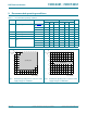
6. Pinning information
6.1 Pinning
6.2 Pin description
(1) This is not a supply pin. The substrate is attached to this
pad using conductive die attach material. There is no
electrical or mechanical requirement to solder this pad.
However, if it is soldered, the solder land should remain
floating or be connected to V
CC
.
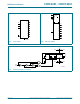
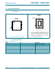
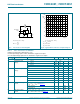
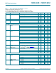
Fig 5. Pin configuration SO16, and (T)SSOP16 Fig 6. Pin configuration DHVQFN16
< 9
&&
< <
=<
< <
< <
(6
9
((
6
*1' 6
DDG
+&
+&7
DDG
9
((
6
(6
< <
< <
=<
< <
*1'
6
<
9
&&
7UDQVSDUHQWWRSYLHZ
WHUPLQDO
LQGH[DUHD
9
&&
+&
+&7
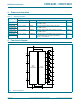
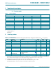
Table 2. Pin description
Symbol Pin Description
E
6 enable input (active LOW)
V
EE
7 supply voltage
GND 8 ground supply voltage
S0, S1, S2 11, 10, 9 select input
Y0, Y1, Y2, Y3, Y4, Y5, Y6, Y7 13, 14, 15, 12, 1, 5, 2, 4 independent input or output
Z 3 common output or input
V
CC
16 supply voltage