
Data Sheet

MLX90640 32x24 IR array
Datasheet
Page 9 of 60
REVISION 11 – 3 AUGUST 2018
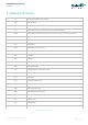
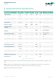
8. General Electrical Specifications
Electrical Parameter Symbol Min. Typ. Max. Unit Condition
Supply Voltage
V
DD
3
3.3
3.6
V
Supply Current
I
DD
1
5
20
25
mA
POR level up analog
V
POR_UP
2.2
2.6
V
VDD rising
POR
level down analog
V
POR_
DOWN
2.55
V
VDD falling
POR hysteresis
V
POR_
hys
50
m
V
Default I
2
C address
0x01
0x33
0xFF
Input high voltage
(SDA, SCL)
V
IH
0.7*V
DD
V Over Ta and V
DD
Input low voltage
(SDA, SCL)
V
LOW
0.3*V
DD
V Over Ta and V
DD
SDA output low voltage V
OL
0.4 V
Over Ta and V
DD
I
SINK
=3mA
SDA leakage
I
SDA_leak
±
10
µA
V
SDA
=3.6V, Ta=
8
5°C
SCL leakage
I
SCL_leak
±
10
µA
V
SCL
=3.6V, Ta=
85
°C
SDA capacitance
C
SDA
10
pF
SCL capacitance
C
SCL
10
pF
Acknowledge
setup time
T
SUAC(MD)
0.45
µs
Acknowledge hold time
T
D
UAC(MD)
0.45
µs
Acknowledge setup time
T
SUAC
(S
D)
0.45
µs
Acknowledge hold time
T
D
UAC(
S
D)
0.45
µs
I
2
C
clock frequency
F
I2C
0.4
1
MHz
EEPROM e
rase/write cycles
10
times
Write cell time
T
WRITE
5
ms
Table 5 Electrical specification
NOTE: For best performance it is recommended to keep the supply voltage as accurate and stable as possible to 3.3V ±
0.1V
NOTE 2: When a data in EEPROM cell to be changed an erase (write 0x0000) must be done prior to writing the new
value. After each write at least 5ms delay is needed in order to writing process to take place.
NOTE 3: Slave address 0x00 must be avoided.