
Data Sheet

MLX90640 32x24 IR array
Datasheet
Page 8 of 60
REVISION 11 – 3 AUGUST 2018
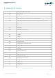
6. Pin Definitions and Descriptions
Pin #
Name
Description
1
SDA
I
2
C
serial data
(input / output)
2
VDD
Positive supply
3
GND
Negative supply (Ground)
4
SCL
I
2
C
serial clock
(input only)
Table 3 Pin definition
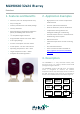
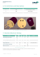
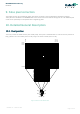
Figure 2 MLX90640 Overview and pin description
7. Absolute Maximum Ratings
Parameter Symbol Min. Typ. Max. Unit Remark
Supply Voltage
(over voltage)
V
DD
5
V
Supply Voltage
(operating max voltage)
V
DD
3.6
Reverse Voltage
(each pin)
-
0.3
V
Operating Temperature
T
AMB
-
40
+
8
5
°C
Storage Temperature
T
ST
-
40
+1
25
°C
Not in plastic tubes
ESD sensitivity (AEC Q100 002)
4
k
V
SDA DC sink current
40
mA
Table 4 Absolute maximum ratings
Exceeding the absolute maximum ratings may cause permanent damage. Exposure to absolute maximum-rated
conditions for extended periods may affect device reliability.