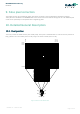
MLX90640 32x24 IR array Datasheet 1. Features and Benefits 2. Application Examples Small size, low cost 32x24 pixels IR array High precision non-contact temperature measurements Easy to integrate Industry standard four lead TO39 package Factory calibrated Noise Equivalent Temperature Difference (NETD) 0.1K RMS @1Hz refresh rate I2C compatible digital interface Programmable refresh rate 0.5Hz…64Hz 3.
MLX90640 32x24 IR array Datasheet Contents 1. Features and Benefits ................................................................ ................................................................................................ ............................................................................................ ............................................................ 1 2. Application Examples................................................................ .....................................
MLX90640 32x24 IR array Datasheet 11.1.9. Restoring corner temperatures (common for all pixel).......................................................... 26 11.1.10. Restoring the KsTo coefficient (common for all pixels) ........................................................ 27 11.1.11. Restoring sensitivity correction coefficients for each temperature range ......................... 27 11.1.12. Restoring the Sensitivity ....................................................................................
MLX90640 32x24 IR array Datasheet Tables Table 1 Ordering information .......................................................................................................................................................... 6 Table 2 Glosarry of terms ................................................................................................................................................................ 7 Table 3 Pin definition ........................................................................
MLX90640 32x24 IR array Datasheet Figure 28 Mechanical drawing of 110° FOV device ..........................................................................................................................
MLX90640 32x24 IR array Datasheet 4.
MLX90640 32x24 IR array Datasheet 5.
MLX90640 32x24 IR array Datasheet 6. Pin Definitions and Descriptions Pin # Name Description 1 SDA I2C serial data (input / output) 2 VDD Positive supply 3 GND Negative supply (Ground) 4 SCL I2C serial clock (input only) Table 3 Pin definition Figure 2 MLX90640 Overview and pin description 7. Absolute Maximum Ratings Parameter Symbol Min. Typ. Max. Unit V Supply Voltage (over voltage) VDD 5 Supply Voltage (operating max voltage) VDD 3.
MLX90640 32x24 IR array Datasheet 8. General Electrical Specifications Electrical Parameter Symbol Min. Typ. Max. Unit Supply Voltage VDD 3 3.3 3.6 V Supply Current IDD 15 20 25 mA VPOR_UP 2.2 2.6 V VDD rising 2.55 V VDD falling POR level up analog POR level down analog POR hysteresis VPOR_DOWN VPOR_hys 50 Default I2C address 0x01 Input high voltage (SDA, SCL) VIH Input low voltage (SDA, SCL) VLOW SDA output low voltage 0x33 Condition mV 0xFF V Over Ta and VDD 0.
MLX90640 32x24 IR array Datasheet 9. False pixel correction The imager can have up to 4 defective pixels, with either no output or out of specification temperature reading. 2 These pixels are identified in the EEPROM table of the sensor and can be read out through the I C. The defective pixel result can be replaced by an interpolation of its neighboring pixels. 10. Detailed General Description 10.1. Pixel position Col 3 Col 2 Col 1 Col 32 The array consists of 768 IR sensors (also called pixels).
MLX90640 32x24 IR array Datasheet 10.2. Communication protocol 2 The device use I C protocol with support of FM+ mode (up to 1MHz clock frequency) and can be only slave on the bus. 2 The SDA and SCL ports are 5V tolerant and the sensor can be directly connected to a 5V I C network. The slave address is programmable and can have up to 127 different slave addresses. 10.2.1. Low level 10.2.1.1.
MLX90640 32x24 IR array Datasheet 10.3. Measurement mode In this mode the measurements are constantly running. Depending on the selected frame rate Fps in the control register, the data for IR pixels and Ta will be updated in the RAM each second. In this mode the external microcontroller has full access to the internal registers and memories of the device. 10.4. Refresh rate The refresh rate is configured by “Control register 1” (0x800D) i.e.
MLX90640 32x24 IR array Datasheet 10.5. Measurement flow Following measurement flow is recommended: Measurement Flow 0.5 Hz 1 Hz 2 Hz POR Wait 80ms + delay determined by the refresh rate Just once after POR 64 Hz 4 sec 2 sec 1 sec …. 0.
MLX90640 32x24 IR array Datasheet 10.6. Reading patterns The array frame is divided in two subpages and depending of bit 12 in “Control register 1” (0x800D) – “Reading pattern” there are two modes of the pixel arrangement: Chess pattern mode (factory default) TV interleave mode NOTE1: As a standard the MLX90640 is calibrated in Chess pattern mode, this results in better fixed pattern noise behaviour of the sensor when in chess pattern mode. For best results Melexis advices to use chess pattern mode.
MLX90640 32x24 IR array Datasheet Subpage 0 --> 0x8000 = 0xXXX8 0x0400 Subpage 1 --> 0x8000 = 0xXXX9 1 2 3 4 5 6 7 8 9 10 11 12 13 14 15 16 17 18 19 20 21 22 23 24 25 26 27 28 29 30 31 32 0x0400 1 2 3 4 5 6 7 8 9 10 11 12 13 14 15 16 17 18 19 20 21 22 23 24 25 26 27 28 29 30 31 32 0x0420 33 34 35 36 37 38 39 40 41 42 43 44 45 46 47 48 49 50 51 52 53 54 55 56 57 58 59 60 61 62 63 64 0x0420 33 34 35 36 37 3
MLX90640 32x24 IR array Datasheet 10.7. Address map 0x0000 ROM 0x03FF 0x0400 RAM 0x07FF 0x2400 EEPROM 0x273F 0x8000 Registers (MLX reserved) 0x800C 0x800D Registers 0x8010 0x8011 Registers (MLX reserved) 0x8016 Figure 10 MXL90640 memory map 10.7.1.
MLX90640 32x24 IR array B7 B6 B5 B4 B3 B2 B1 B0 Enable subpages mode B8 Melexis reserved B9 Enable data hold B10 Select subpage B11 Reading pattern B12 Refresh rate control B13 Resolution control B14 Melexis reserved B15 Enable subpages repeat Datasheet 0 - - - Transfer the data into storage RAM only if en_overwrite = 1 (check 0x8000) 0 Toggles between subpage "0" and subpage "1" if Enable subpages mode = "1" (default) 1 Select subpage determines which subpage to be measured
MLX90640 32x24 IR array B3 B2 B1 B0 B7 B6 B5 B4 B3 B2 B1 B0 FM+ disable B4 I2C threshold levels B5 SDA driver current limit control B6 Melexis reserved B7 Melexis reserved Datasheet 0 - - - - - - - - - - - - I2C configuration register - 0x800F 0 FM+ mode enabled (default) 1 FM+ mode disabled 0 VDD reffered threshold (normal mode) (default) 1 1.8V reffered threshold (1.
MLX90640 32x24 IR array Datasheet 10.7.3.
MLX90640 32x24 IR array Datasheet Address 0x2400 0x2410 0x2420 0x2430 0x2440 0x2450 0x2460 0x2470 0x2480 0x2490 0x24A0 0x24B0 0x24C0 0x24D0 0x24E0 0x24F0 0x2500 0x2510 0x2520 0x2530 0x2540 0x2550 0x2560 0x2570 0x2580 0x2590 0x25A0 0x25B0 0x25C0 0x25D0 0x25E0 0x25F0 0x2600 0x2610 0x2620 0x2630 0x2640 0x2650 0x2660 0x2670 0x2680 0x2690 0x26A0 0x26B0 0x26C0 0x26D0 0x26E0 0x26F0 0x2700 0x2710 0x2720 0x2730 0 1 2 3 4 5 6 7 8 9 A B Osc Trim Ana Trim MLX Conf reg MLX MLX MLX ID 1 ID 2 ID 3
MLX90640 32x24 IR array Datasheet Address \ bit 0x2410 0x2411 0x2412 0x2413 0x2414 0x2415 0x2416 0x2417 0x2418 0x2419 0x241A 0x241B 0x241C 0x241D 0x241E 0x241F 0x2420 0x2421 0x2422 0x2423 0x2424 0x2425 0x2426 0x2427 0x2428 0x2429 0x242A 0x242B 0x242C 0x242D 0x242E 0x242F 0x2430 0x2431 0x2432 0x2433 0x2434 0x2435 0x2436 0x2437 0x2438 0x2439 0x243A 0x243B 0x243C 0x243D 0x243E 0x243F 0x2440 0x2441 … 0x245E 0x245F 0x2460 0x2461 … 0x273E 0x273F 15 14 13 12 11 10 9 8 7 6 5 4 scale_Occ_col 3 2 1
MLX90640 32x24 IR array Datasheet 11. Calculating Object Temperature 11.1. Restoring calibration data from EERPOM NOTE: All data in the EEPROM is coded as two’s complement (unless otherwise noted) In the example we are restoring the calibration data for pixel (12, 16) 11.1.1. Restoring the VDD sensor parameters Following formula is used to calculate the VDD of the sensor: = If = 0 2433 & 0 2 00 > 127 ∗ 2" #$$%" = = 0 2433 & 0 00 #$$%" = (#$$%" − 256) ∗ 2" − 2 − 256 ( 11.1.2.
MLX90640 32x24 IR array Datasheet If #C?D?89 > 32767 #C?D?012 = E Where: #C?D?89 = #C?D?89 − 65536 #C?D? L∗2 #C?D? ∗ AFGℎIC?D? + #JK #C?D? = @AB 0 0720 If #C?D? > 32767 #JK = @AB 0 0700 If #JK > 32767 #JK = #JK − 65536 0 2410 & 0 2% AFGℎIC?D?_KK = AFGℎIC?D? = #C?D? = #C?D? − 65536 000 AFGℎIC?D?_KK +8 2% 11.1.3.
MLX90640 32x24 IR array Datasheet Highlighted in yellow parameters are extracted here after. As a default the device is factory calibrated in Chess pattern mode thus the best performance will be when a Chess pattern is used. However some customers may choose to use the device in interleaved mode which will degrade the device performance. In this case a correction can be applied to restore to some extend the performance. Once the IR data is compensated the calculation for To is done using default flow.
MLX90640 32x24 IR array Datasheet A==R]^38 = KK >p%q%q & >p >>> %38 If A==R]^38 > 7 A==rf*gS1de = A==f]ghij3t = (i.e. the four most significant bits, signed) A==R]^38 = A==R]^38 − 16 KK >p%q%> & >p> >> %s KK >p%q%— & >p >>> %38 If A==f]ghij3t > 7 A==rf*gSadblmn = ’‚wpSg (12,16) = (unsigned) (i.e.
MLX90640 32x24 IR array Datasheet ?*_}`_KK depends on the pixel position in the array i.e.
MLX90640 32x24 IR array Datasheet 11.1.10. Restoring the KsTo coefficient (common for all pixels) X?] = Where: 2 Where: X?]% = X?] _KK ;r.d a0bc X?] a0bc = 0 243F & 0 000F + 8 (unsigned) X?] 0 243D & 0 00FF(signed) _KK = If X?] ;r.d8_šš % 5 .d a0bc _KK > 127 X?] _KK = X?] _KK − 256 Where: X?]%_KK = X?]( = Where: X?]q = Where: 2 %s If X?]%_KK > 127 X?](_KK ;r.d a0bc X?](_KK = 2 KK >p%q(£ & >p˜˜>> X?]%_KK = X?]%_KK − 256 0 243E & 0 00FF(signed) If X?](_KK > 127 X?]q_KK ;r.
MLX90640 32x24 IR array Datasheet 11.1.12. Restoring the Sensitivity Please note that there are two sensitivities for the compensation pixel – one for each subpage ’`C_rh•‚*\S_> = KK >p%q(¬ & >p>( % – a0bc_{- ’`C_rh•‚*\S_ = ’`C_rh•‚*\S_> ∗ „1 + Where: 0 2420 & 0 2% ’rf*gS_`C = =®_®1/®0R*ƒw] = `C_C _C>_R*ƒw] %- 000 KK >p%q(¬ & >p `>> %3v If =®_®1/®0R*ƒw] > 31 † + 27 (signed) =®_®1/®0R*ƒw] = =®_®1/®0R*ƒw] − 64 11.1.13.
MLX90640 32x24 IR array Datasheet ?* a0bc_3 = KK >p%q( Where: ?*{-_šš %u = If & >p>>˜> + 8 (unsigned) (the same one as for the 0 243B & 0 00FF (signed) ?*{-_šš > 127 ?*{-_šš = ?*{-_šš ?*(w,…) coefficients) − 256 11.1.16. Restoring the TGC coefficient )±= = Where: ?²`šš %9 )±=KK = 0 243C & 0 00FF (signed) If )±=KK > 127 )±=KK = )±=KK − 256 NOTE 1: In a MLX90640ESF–BAx–000-TU device, the TGC coefficient is set to 0 and must not be changed.
MLX90640 32x24 IR array Datasheet 11.2. Temperature Calculation 11.2.1. Example Input Data 11.2.1.1.
MLX90640 32x24 IR array Datasheet OCC_rows_10 – 4 bits OCC_rows_09 – 4 bits OCC_rows_10 = -1 OCC_rows_09 = 2 0x2415 OCC_rows_16 – 4 bits OCC_rows_15 – 4 bits OCC_rows_14 – 4 bits OCC_rows_13 – 4 bits 0xE2E2 OCC_rows_16 = -2 OCC_rows_15 = 2 OCC_rows_14 = -2 OCC_rows_13 = 2 0x2416 OCC_rows_20 – 4 bits OCC_rows_19 – 4 bits OCC_rows_18 – 4 bits OCC_rows_17 – 4 bits 0xD1E1 OCC_rows_20 = -3 OCC_rows_19 = 1 OCC_rows_18 = -2 OCC_rows_17 = 1 0x2417 OCC_rows_24 – 4 bits OCC_rows_23 – 4 bits OCC_rows_22 –
MLX90640 32x24 IR array Datasheet OCC_column_30 – 4 bits OCC_column_29 – 4 bits OCC_column_30= 0 OCC_column_29 = 4 0x2420 Alpha scale – 4 bits Scale_ACC_row – 4 bits Scale_ACC_column – 4 bits Scale_ACC_remnand – 4 bits 0x79A6 Alpha scale = 37 Scale_ACC_row = 9 Scale_ACC_column = 10 Scale_ACC_remnand = 6 0x2421 Pix_sensitivity_average - 16 bits 0x2F44 Pix_sensitivity_average = 8.
MLX90640 32x24 IR array Datasheet 0x242B ACC_column_16 – 4 bits ACC_column_15 – 4 bits ACC_column_14 – 4 bits ACC_column_13 – 4 bits 0x3333 ACC_column_16 = 3 ACC_column_15 = 3 ACC_column_14 = 3 ACC_column_13 = 3 0x242C ACC_column_20 – 4 bits ACC_column_19 – 4 bits ACC_column_18 – 4 bits ACC_column_17 – 4 bits 0x2333 ACC_column_20 = 2 ACC_column_19 = 3 ACC_column_18= 3 ACC_column_17 = 3 0x242D ACC_column_24 – 4 bits ACC_column_23 – 4 bits ACC_column_22 – 4 bits ACC_column_21 – 4 bits 0x0112 ACC_c
MLX90640 32x24 IR array Datasheet Alpha_CP_SP_0 – 10 bits Alpha_CP_SP_0 = 4.0745362639427E-09 0x243A CP_off_delta (SP_1 - SP_0) – 6 bits Offset_CP_SP_0 – 10 bits 0xFBB5 CP_off_delta (SP_1 - SP_0) = -2 Offset_CP_SP_0 = -75 0x243B Kv_CP – 8 bits Kta_CP – 8 bits 0x044B Kv_CP = 0.5 Kta_CP = 0.00457763671875 0x243C KsTa – 8 bits TGC – 8 bits 0xF020 KsTa = -0.001953125 TGC = 1 0x243D KsTo2 (0°C…CT3°C) – 8 bits KsTo1 (<0°C) – 8 bits 0x9797 KsTo2 (0°C…CT3°C) = -0.0008010864 KsTo1 (<0°C) = -0.
MLX90640 32x24 IR array Datasheet 11.2.2. Temperature calculation After the parameters restore the temperature calculation is done using following calculation flow (assuming that the EEPROM data are already extracted): Supply voltage value calculation (common for all pixels) - 11.2.2.2 Ambient temperature calculation (common for all pixels) - 11.2.2.3 Gain compensation - 11.2.2.5.1 IR data compensation – offset, VDD and Ta - 11.2.2.5.3 IR data Emissivity compensation - 11.2.2.5.
MLX90640 32x24 IR array Datasheet @YXoF³ZOo•f]RR = %™c dbl2_dnšš %™c dbl2_dn™š´ = %8 %8 =1 In case the ADC resolution is changed the one must multiply the @YXoF³ZOo•f]RR coefficient with the RAM data for VDD only. Please note that the data for Vbe, PTAT and IR pixels (including CP) must not be changed. 11.2.2.2.
MLX90640 32x24 IR array Datasheet @AB 0 072A = 0 ===5 = 52421 ∆# = If 52421 > 32767 @AB 0 072A = 52421 − 65536 = −13115 LSB −13115 − (−13056) −59 = ≈ 0.
MLX90640 32x24 IR array Datasheet Please note that this value is updated every frame and it is the same for all pixels including CP regardless the subpage number 11.2.2.5. Pixel data calculations The pixel addressing is following the pattern as described in Reading pattern shown in Fig 5: 11.2.2.5.1. Gain compensation The first step of the data processing on raw IR data is always the gain compensation, regardless of pixel or subpage number.
MLX90640 32x24 IR array Datasheet oWWXYZ(12,16) = If 2 < 31 GO KK >p%"D >p> D> & >p `>> %3v oWWXYZ(12,16) = 2 V==rf*gS1cmn0n2 = PQ RST (12,16) = & >p `>> %3v = 0 0002 0 2410 & 0 000 = 0 4210 & 0 000 = 0 0000 = 0 = −69 + (−1) ∗ 2% + (−2) ∗ 2 + 2 ∗ 2> = −69 − 4 − 4 + 2 = −75 11.2.2.5.3. IR data compensation – offset, VDD and Ta GO PQ (12, 16) ?*( %, ‹) Where: = \*wj (12,16) = GO − GO PQ RST 5.0(38,3t) _Ãà & v•vvvà ;.0_™{_šš • % = ?*( %, ‹)_KK 8 5.
MLX90640 32x24 IR array Datasheet 11.2.2.5.4. IR data Emissivity compensation Emissivity compensation: For the example we assume Emissivity = 1. Note that the Emissivity coefficient is user defined and it is not stored in the device EEPROM) #Ä}( %, ‹)šm_ _Å_2Æ_{ÇÈ-šÉÊ/.šË = ‚wpÇÊ ( %, ‹) Ì = ¸>>. %q¬"‹¬> ¸¸ = 700.882495690877 11.2.2.6. CP data calculations 11.2.2.6.1.
MLX90640 32x24 IR array Datasheet VWW_=®rh•‚*\S_ Where: _ Sgƒ* If 62 > 31 ?*{- = ;.0{-_šš % 5.0 a0bc ?* a0bc_3 ;,{-_šš 5 % , a0bc = = a0bc_3 ?*{-_šš = KK >p%q(D & >p `>> %3v VWW_=®rh•‚*\S_ = _ Sgƒ* VWW_=®rh•‚*\S_ = −75 + (−2) = −77 Where: {- = {-_šš = = q %| %s = %3v = 0 003 = 62 = 62 − 64 = −2 = 0.
MLX90640 32x24 IR array Datasheet GO YFjhi•SR − 1 O•Z E L GO YFjhi•SR − 1 32 ®IZZY•• = ÎO•Z E L − O•Z Î Ï ∗ 2Ï 32 2 Where the O•Z function is giving the truncated whole number without fractional component of the result. Where o• is exclusive or or exclusive disjunction is a logical operation that outputs true only when inputs differ.
MLX90640 32x24 IR array Datasheet 11.2.2.8. Normalizing to sensitivity ’f]i‚( %, ‹) = +’( ’`C_rh•‚*\S_> = %, ‹) − )±= ∗ E(1 − ®IZZY••) ∗ ’`C = KK >p%q(¬ & >p>( % – a0bc_{- = >pKqq‹ & >p>( ’`C_rh•‚*\S_ = ’`C_rh•‚*\S_> ∗ „1 + % – a0bc_{- `C_C _C>102_d † %- ’`C_rh•‚*\S_ = 3.85171006200835 − 09 Where: 0 2420 & 0 2% ’rf*gS_`C = =®_®1_®0R*ƒw] = X?* = ;r.
MLX90640 32x24 IR array Datasheet ’( A==rf*gS1cmn0n2 = = %, ‹) ’f]i‚( ’f]i‚( % >>•(∗%À •(∗%3v • >∗%t %, ‹) %, ‹) ’f]i‚( = +’( %|- %, ‹) 0 2420 & 0 000F = 0 79A6 & 0 000F = 0 0006 = 6 = 1.26223312690854 − 07 − )±= ∗ E(1 − ®IZZY••) ∗ ’`C lŒ 0«cv + ®IZZY•• ∗ ’`C_rh•‚*\S_ L: ∗ ‡1 + r?* ∗ ()* − )*> )ˆ = „1.26223312690854 − 07 − 1 ∗ ‡(1 − 0) ∗ 4.07453626394272 − 09 + 0 ∗ 3.85171006200835 − 09ˆ† ∗ ‡1 + −0.001953125 ∗ (39.184 − 25)ˆ %, ‹) = 1.1876487360496 − 07 11.2.2.9.
MLX90640 32x24 IR array Datasheet 11.2.2.9.1. Calculations for extended temperature ranges In order to extent the object temperature range and get the best possible accuracy an additional calculation cycle is needed.
MLX90640 32x24 IR array Datasheet X?]q = Where: 2 If X?](_KK > 127 X?]q_KK ;r.d a0bc = X?]q_KK = X?](_KK = X?](_KK − 256 = 151 − 256 = −105 −105 = −0.00080108642578125 2¸ KK >p%q(› & >p>>˜˜ %s If X?]q_KK > 127 = >p¬¸¬¸ & >p˜˜>> %s = 0 0097 = 151 (signed) X?]q_KK = X?]q_KK − 256 = 151 − 256 = −105 Now we can calculate sensitivity correction coefficients for each temperature range: AFGℎIf]RR10n«c3 = 1 „1 + X)o1 ∗ ‡0 − (−40)ˆ† AFGℎIf]RR10n«c8 = 1 = 1 „1 − 0.
MLX90640 32x24 IR array Datasheet 12. Performance graphs 12.1. Accuracy All accuracy specifications apply under settled isothermal conditions only. Furthermore, the accuracy is only valid if the object fills the FOV of the sensor completely.
MLX90640 32x24 IR array Datasheet Zone 3 Zone 3 Zone 1 Zone 3 Zone 2 MLX90640BAA Zone 1 Zone 3 Zone 2 MLX90640BAB Figure 18 Different accuracy zones depending on device type (BAA on the left and BAB on the right) REVISION 11 – 3 AUGUST 2018 Page 48 of 60
MLX90640 32x24 IR array Datasheet Startup time 12.1.1. First valid data After POR the first valid data is available after (depending on the selected refresh rate) )[*gw )[*gw _ *ƒ* = 40 + 500, ms _ *ƒ* which is calculated as: (Example refresh rate is 2Hz – the default value) It is always subpage 0 to be measured first after POR then subpage 1 and so on alternating.
MLX90640 32x24 IR array Datasheet 12.2. Noise performance and resolution There are two bits in the configuration register that allow changing the resolution of the MLX90640 measurements. Increasing the resolution decreases the quantization noise and improves the overall noise performance.
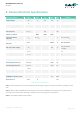
MLX90640 32x24 IR array Datasheet Figure 22 MLX90640BAB noise vs pixel and refresh rate at 1Hz and 2Hz Figure 23 MLX90640BAB noise vs pixel and refresh rate at 4Hz, 8Hz and 16Hz NETD (K) 1Hz RMS noise (temperature equivalent), all pixels MLX90640 Average Min Standard deviation BAA 0.14 0.1 0.05 BAB 0.25 0.2 0.
MLX90640 32x24 IR array Datasheet 12.3. Field of view (FOV) Point heat source Sensitivity 100% 50% Field Of View Angle of incidence Rotated sensor Figure 24: Field Of View measurement The specified FOV is calculated for the wider direction, in this case for the 32 pixels.
MLX90640 32x24 IR array Datasheet 13. Application information 13.1. Electrical considerations Figure 25 MLX90640 electrical connections As the MLX90640Bxx is fully I2C compatible it allows to have a system in which the MCU may be supplied with VDD=2.6V…5V while the sensor it’s self is supplied from separate supply VDD1=3.3V (or even left with no supply i.e. VDD=0V), with the I2C connection running at supply voltage of the MCU.
MLX90640 32x24 IR array Datasheet 13.2. Using the device in “image mode” In some applications may not be necessary to calculate the temperature but rather to have just and image (for instance in machine vision systems). In this case it is not necessary to carry out all calculations which would save computation time or allow the one to use weaker CPU. In order to get thermal image only following computation flow is to be used: Supply voltage value calculation (common for all pixels) - 11.2.2.
MLX90640 32x24 IR array Datasheet Power dissipation within the package may affect performance in two ways: by heating the “ambient” sensitive element significantly beyond the actual ambient temperature, as well as by causing gradients over the package that will inherently cause thermal gradient over the cap Power supply decoupling capacitor is needed as with most integrated circuits. MLX90640Bxx is a mixed-signal device with sensors, small signal analog part, digital part and I/O circuitry.
MLX90640 32x24 IR array Datasheet 15. Mechanical drawings 15.1.
MLX90640 32x24 IR array Datasheet 15.2.
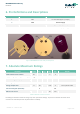
MLX90640 32x24 IR array Datasheet 15.3. Device marking The MLX90640 is laser marked with 10 symbols as follows. 0 A A xxxxx xx Laser marking 2 digits Split number 5 digits LOT number 0 A FOV = 110° B FOV = 55° A Device without thermal gradient compensation (TGC = 0 and may not be changed) C Device with thermal gradient compensation (TGC = -4…+3.98) MLX90640 Example: “0CA1010218” – Device type MLX90640BAA from lot 10102, sub LOT split 18 and Thermal Gradient Compensation activated.
MLX90640 32x24 IR array Datasheet 16. Standard Information Our products are classified and qualified regarding soldering technology, solderability and moisture sensitivity level according to standards in place in Semiconductor industry. For further details about test method references and for compliance verification of selected soldering method for product integration, Melexis recommends reviewing on our web site the General Guidelines soldering recommendation.
MLX90640 32x24 IR array Datasheet 11/04/2018 Updated accuracy table including BAB version, CP for different subpages, compensation for different reading patterns, extended temperature ranges calculations. 03/08/2018 Added: github driver link, ESD = 2kV 4kV, Step mode removed, Internal register tables updated Table 16 Revision history 19. Contact For the latest version of this document, go to our website at www.melexis.com.