
Data Sheet
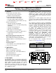

DRV2605L
SLOS854C –MAY 2014–REVISED SEPTEMBER 2014
www.ti.com
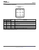
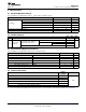
6.5 Electrical Characteristics
T
A
= 25°C, V
DD
= 3.6 V (unless otherwise noted)
PARAMETER TEST CONDITIONS MIN TYP MAX UNIT
V
(REG)
Voltage at the REG pin 1.83 V
EN, IN/TRIG, SDA, SCL
I
IL
Digital low-level input current 1 µA
V
DD
= 5.2 V , V
I
= 0 V
IN/TRIG, SDA, SCL
1
V
DD
= 5.2 V, V
I
= V
DD
I
IH
Digital high-level input current µA
EN
3.5
V
DD
= 5.2 V, V
I
= V
DD
V
OL
Digital low-level output voltage SDAI
OL
= 4 mA 0.4 V
EN
R
(EN-GND)
Digital pull-down resistance 2 MΩ
V
DD
= 5.2 V , V
I
= V
DD
I
(SD)
Shutdown current V
(EN)
= 0 V 4 7 µA
I
I(standby)
Standby current V
(EN)
= 1.8 V, STANDBY = 1 4.1 7 µA
I
Q
Quiescent current V
(EN)
= 1.8 V, STANDBY = 0, no signal 0.5 0.65 mA
Z
I
Input impedance IN/TRIG to V
(CM_ANA)
100 kΩ
IN/TRIG common-mode voltage
V
(CM_ANA)
AC_COUPLE = 1 0.9 V
(AC-coupled)
Z
O(SD)
Output impedance in shutdown OUT+ to GND, OUT– to GND 15 kΩ
Load impedance threshold for
Z
L(th)
OUT+ to GND, OUT– to GND 4 Ω
over-current detection
Duty cycle = 90%, LRA mode, no load 2.4 3.5
Average battery current during
I
(BAT_AV)
mA
operation
Duty cycle = 90%, ERM mode, no load 2.3 3.5
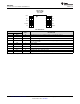
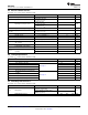
6.6 Timing Requirements
T
A
= 25°C, V
DD
= 3.6 V (unless otherwise noted)
MIN NOM MAX UNIT
ƒ
(SCL)
Frequency at the SCL pin with no wait states 400 kHz
t
w(H)
Pulse duration, SCL high 0.6 µs
t
w(L)
Pulse duration, SCL low 1.3 µs
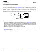
See Figure 1.
t
su(1)
Setup time, SDA to SCL 100 ns
t
h(1)
Hold time, SCL to SDA 10 ns
Bus free time between stop and start
t
(BUF)
1.3 µs
condition
t
su(2)
Setup time, SCL to start condition 0.6 µs
See Figure 2.
t
h(2)
Hold time, start condition to SCL 0.6 µs
t
su(3)
Setup time, SCL to stop condition 0.6 µs
6.7 Switching Characteristics
T
A
= 25°C, V
DD
= 3.6 V (unless otherwise noted)
PARAMETER TEST CONDITIONS MIN TYP MAX UNIT
Time from the GO bit or external trigger
0.7
command to output signal
t
(start)
Start-up time ms
Time from EN high to output signal
1.5
(PWM/Analog Modes)
ƒ
O(PWM)
PWM Output Frequency 19.5 20.5 21.5 kHz
6 Submit Documentation Feedback Copyright © 2014, Texas Instruments Incorporated
Product Folder Links: DRV2605L