
Data Sheet
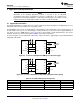
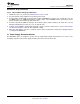

REG
SCL
SDA
IN/TRIG
EN
VDD
OUT-
GND
OUT+
VDD/NC
C
(REG)
C
(VDD)
Via
Via should connect
to a ground plane
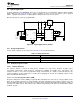
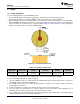
C
(REG)
C
(VDD)
V
DD
REG OUT+
GND
OUTt
SDA
IN
SCL
EN
Via
Via should connect
to a ground plane
DRV2605L
www.ti.com
SLOS854C –MAY 2014–REVISED SEPTEMBER 2014
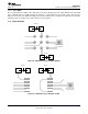
11.1.1 Trace Width
The recommended trace width at the solder pins is 75 µm to 100 µm to prevent solder wicking onto wider PCB
traces. Maintain this trace width until the pin pattern is escaped then the trace width can be increased for
improved current flow. The width and length of the 75-µm to 100-µm traces should be as symmetrical as possible
around the device to provide even solder reflow on each of the pins.
11.2 Layout Example
Figure 66. DRV2605L Layout Example DSBGA
Figure 67. DRV2605L Layout Example VSSOP
Copyright © 2014, Texas Instruments Incorporated Submit Documentation Feedback 59
Product Folder Links: DRV2605L