
Data Sheet

DRV2605L
www.ti.com
SLOS854C –MAY 2014–REVISED SEPTEMBER 2014
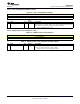
8.6.27 V
(BAT)
Voltage Monitor (Address: 0x21)
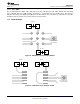
Figure 56. V
(BAT)
Voltage-Monitor Register
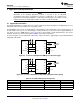
7 6 5 4 3 2 1 0
VBAT[7:0]
R/W-0
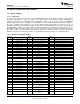
Table 30. V
(BAT)
Voltage-Monitor Register Field Descriptions
BIT FIELD TYPE DEFAULT DESCRIPTION
7-0 VBAT[7:0] R/W 0
This bit provides a real-time reading of the supply voltage at the V
DD
pin. The
device must be actively sending a waveform to take a reading.
V
DD
(V) = VBAT[7:0] × 5.6V / 255
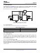
8.6.28 LRA Resonance Period (Address: 0x22)
Figure 57. LRA Resonance-Period Register
7 6 5 4 3 2 1 0
LRA_PERIOD[7:0]
R/W-0
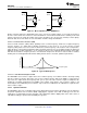
Table 31. LRA Resonance-Period Register Field Descriptions
BIT FIELD TYPE DEFAULT DESCRIPTION
7-0 LRA_PERIOD[7:0] R/W 0
This bit reports the measurement of the LRA resonance period. The device must
be actively sending a waveform to take a reading.
LRA period (us) = LRA_Period[7:0] × 98.46 µs
Copyright © 2014, Texas Instruments Incorporated Submit Documentation Feedback 51
Product Folder Links: DRV2605L