
Data Sheet

DRV2605L
SLOS854C –MAY 2014–REVISED SEPTEMBER 2014
www.ti.com
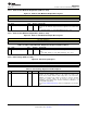
8.6.25 Control5 (Address: 0x1F)
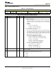
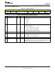
Figure 54. Control5 Register
7 6 5 4 3 2 1 0
AUTO_OL_CNT[1:0] LRA_AUTO_O PLAYBACK_IN BLANKING_TIME[3:2] IDISS_TIME[3:2]
PEN_LOOP TERVAL
R/W-1 R/W-0 R/W-0 R/W-0 RW-0 RW-0 RW-0
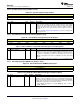
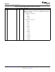
Table 28. Control5 Register Field Descriptions
BIT FIELD TYPE DEFAULT DESCRIPTION
7-6 AUTO_OL_CNT[1:0] R/W 2
This bit selects number of cycles required to attempt synchronization before
transitioning to open loop when the LRA_AUTO_OPEN_LOOP bit is asserted,
0: 3 attempts
1: 4 attempts
2: 5 attempts
3: 6 attempts
5 LRA_AUTO_OPEN_LOOP R/W 0
This bit selects the automatic transition to open-loop drive when a back-EMF
signal is not detected (LRA only).
0: Never transitions to open loop
1: Automatically transitions to open loop
4 PLAYBACK_INTERVAL R/W 0
This bit selects the memory playback interval.
0: 5 ms
1: 1 ms
3-2 BLANKING_TIME[3:2] R/W 0
This bit sets the MSB for the BLANKING_TIME[3:0]. See the
BLANKING_TIME[3:0] bit in the Control2 (Address: 0x1C) section for details.
Advanced use only.
1-0 IDISS_TIME[3:2] R/W 0
This bit sets the MSB for IDISS_TIME[3:0]. See the IDISS_TIME[1:0] bit in the
Control2 (Address: 0x1C) section for details. Advanced use only.
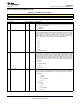
8.6.26 LRA Open Loop Period (Address: 0x20)
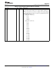
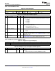
Figure 55. LRA Open Loop Period Register
7 6 5 4 3 2 1 0
Reserved OL_LRA_PERIOD[6:0]
R/W-0
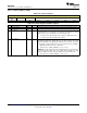
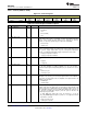
Table 29. LRA Open Loop Period Register Field Descriptions
BIT FIELD TYPE DEFAULT DESCRIPTION
7-0 OL_LRA_PERIOD[6:0] R/W 0
This bit sets the period to be used for driving an LRA when open-loop mode is
selected.
LRA open-loop period (µs) = OL_LRA_PERIOD[6:0] × 98.46 µs
50 Submit Documentation Feedback Copyright © 2014, Texas Instruments Incorporated
Product Folder Links: DRV2605L