
Data Sheet

DRV2605L
www.ti.com
SLOS854C –MAY 2014–REVISED SEPTEMBER 2014
6 Specifications
6.1 Absolute Maximum Ratings
over operating free-air temperature range, T
A
= 25°C (unless otherwise noted)
MIN MAX UNIT
V
DD
–0.3 5.5 V
EN –0.3 V
DD
+ 0.3 V
Input voltage SDA –0.3 V
DD
+ 0.3 V
SCL –0.3 V
DD
+ 0.3 V
IN/TRIG –0.3 V
DD
+ 0.3 V
Operating free-air temperature range, T
A
–40 85 °C
Operating junction temperature range, T
J
–40 150 °C
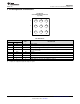
6.2 Handling Ratings
MIN MAX UNIT
T
stg
Storage temperature range –65 150 °C
DSBGA package, all pins –1000 1000
Human body model (HBM), per
OUT+, OUT– –500 500
Electrostatic
ANSI/ESDA/JEDEC JS-001
V
(ESD)
VSSOP package V
discharge
Other pins –1000 1000
Charged device model (CDM), per JEDEC specification JESD22-C101, all pins –250 250
6.3 Recommended Operating Conditions
over operating free-air temperature range (unless otherwise noted)
MIN MAX UNIT
V
DD
Supply voltage V
DD
2 5.2 V
ƒ
(PWM)
PWM input frequency IN/TRIG Pin 10 250 kHz
Z
L
Load impedance V
DD
= 5.2 V 8 Ω
V
IL
Digital low-level input voltage EN, IN/TRIG, SDA, SCL 0.5 V
V
IH
Digital high-level input voltage EN, IN/TRIG, SDA, SCL 1.3 V
V
I(ANA)
Input voltage (analog mode) IN/TRIG 0 1.8 V
ƒ
(LRA)
LRA Frequency Range 125 300 Hz
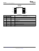
6.4 Thermal Information
DSBGA
THERMAL METRIC
(1)
UNIT
(9-PINS)
R
θJA
Junction-to-ambient thermal resistance 145.2
R
θJC(top)
Junction-to-case (top) thermal resistance 0.9
R
θJB
Junction-to-board thermal resistance 105
°C/W
ψ
JT
Junction-to-top characterization parameter 5.1
ψ
JB
Junction-to-board characterization parameter 103.3
R
θJC(bot)
Junction-to-case (bottom) thermal resistance —
(1) For more information about traditional and new thermal metrics, see the IC Package Thermal Metrics application report, SPRA953.
Copyright © 2014, Texas Instruments Incorporated Submit Documentation Feedback 5
Product Folder Links: DRV2605L