
Data Sheet

DRV2605L
www.ti.com
SLOS854C –MAY 2014–REVISED SEPTEMBER 2014
8.6.24 Control4 (Address: 0x1E)
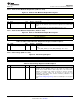
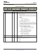
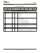
Figure 53. Control4 Register
7 6 5 4 3 2 1 0
ZC_DET_TIME[ ZC_DET_TIME[ AUTO_CAL_TIME[1:0] Reserved OTP_STATUS Reserved OTP_PROGRA
1] 0] M
R/W-0 R/W-0 R/W-1 R/W-0 R-0 R/W-0
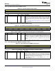
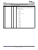
Table 27. Control4 Register Field Descriptions
BIT FIELD TYPE DEFAULT DESCRIPTION
7-6 ZC_DET_TIME[1:0] R/W 0
This bit sets the minimum length of time devoted for detecting a zero crossing
(advanced use only).
0: 100 µs
1: 200 µs
2: 300 µs
3: 390 µs
5-4 AUTO_CAL_TIME[1:0] R/W 2
This bit sets the length of the auto calibration time. The AUTO_CAL_TIME[1:0]
bit should be enough time for the motor acceleration to settle when driven at the
RATED_VOLTAGE[7:0] value.
0: 150 ms (minimum), 350 ms (maximum)
1: 250 ms (minimum), 450 ms (maximum)
2: 500 ms (minimum), 700 ms (maximum)
3: 1000 ms (minimum), 1200 ms (maximum)
3 Reserved
2 OTP_STATUS R 0
OTP Memory status
0: OTP Memory has not been programmed
1: OTP Memory has been programmed
1 Reserved
0 OTP_PROGRAM R/W 0
This bit launches the programming process for one-time programmable (OTP)
memory which programs the contents of register 0x16 through 0x1A into
nonvolatile memory. This process can only be executed one time per device.
See the Programming On-Chip OTP Memory section for details.
Copyright © 2014, Texas Instruments Incorporated Submit Documentation Feedback 49
Product Folder Links: DRV2605L