
Data Sheet


DRV2605L
SLOS854C –MAY 2014–REVISED SEPTEMBER 2014
www.ti.com
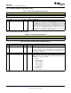
8.6.11 Audio-to-Vibe Control (Address: 0x11)
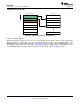
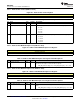
Figure 40. Audio-to-Vibe Control Register
7 6 5 4 3 2 1 0
Reserved ATH_PEAK_TIME[1:0] ATH_FILTER[1:0]
R/W-0 R/W-1 R/W-0 R/W-1
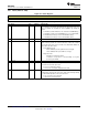
Table 14. Audio-to-Vibe Control Register Field Descriptions
BIT FIELD TYPE DEFAULT DESCRIPTION
7-4 Reserved
3-2 ATH_PEAK_TIME[1:0] R/W 1
This bit sets the peak detection time for the audio-to-vibe signal path:
0: 10 ms
1: 20 ms
2: 30 ms
3: 40 ms
1-0 ATH_FILTER[1:0] R/W 1
This bit sets the low-pass filter frequency for the audio-to-vibe signal path:
0: 100 Hz
1: 125 Hz
2: 150 Hz
3: 200 Hz
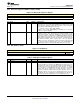
8.6.12 Audio-to-Vibe Minimum Input Level (Address: 0x12)
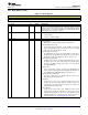
Figure 41. Audio-to-Vibe Minimum Input Level Register
7 6 5 4 3 2 1 0
ATH_MIN_INPUT[7:0]
R/W-0 R/W-0 R/W-0 R/W-1 R/W-1 R/W-0 R/W-0 R/W-1
LEGEND: R/W = Read/Write; R = Read only; -n = value after reset
Table 15. Audio-to-Vibe Minimum Input Level Register Field Descriptions
BIT FIELD TYPE DEFAULT DESCRIPTION
7-0 ATH_MIN_INPUT[7:0] R/W 0x19
This bit sets the minimum voltage level at the IN/TRIG pin that is detected by
the audio-to-vibe engine. Levels below this are ignored.
ATH_MIN_INPUT Voltage (V
PP
) = ATH_MIN_INPUT[7:0] × 1.8 V / 255
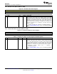
8.6.13 Audio-to-Vibe Maximum Input Level (Address: 0x13)
Figure 42. Audio-to-Vibe Maximum Input Level Register
7 6 5 4 3 2 1 0
ATH_MAX_INPUT[7:0]
R/W-1
Table 16. Audio-to-Vibe Maximum Input Level Register Field Descriptions
BIT FIELD TYPE DEFAULT DESCRIPTION
7-0 ATH_MAX_INPUT[7:0] R/W 0xFF
This bit sets the full-scale voltage level at the IN/TRIG pin for audio-to-vibe
mode.
ATH_MAX_INPUT Voltage (V
PP
) = ATH_MAX_INPUT[7:0] × 1.8 V / 255
40 Submit Documentation Feedback Copyright © 2014, Texas Instruments Incorporated
Product Folder Links: DRV2605L