
Data Sheet
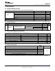

EN
OUT+
SCL
IN/TRIG
SDA GND
OUT±
REG
A
B
C
32
1
V
DD
DRV2605L
www.ti.com
SLOS854C –MAY 2014–REVISED SEPTEMBER 2014
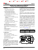
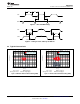
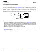
5 Pin Configuration and Functions
YZF Package
9-Pin DSBGA With 0,5-mm Pitch
(Top View)
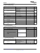
Pin Functions
PIN
TYPE
(1)
DESCRIPTION
NO. NAME
A1 EN I Device enable
A2 REG O The REG pin is the 1.8-V regulator output. A 1-µF capacitor is required.
A3 OUT+ O Positive haptic driver differential output
Multi-mode Input. I
2
C selectable as PWM, analog, or trigger. If not used, this pin should
B1 IN/TRIG I
be connected to GND
B2 SDA I/O I
2
C data
B3 GND P Supply ground
C1 SCL I I
2
C clock
C3 OUT– O Negative haptic-driver differential output
C2 V
DD
P Supply input (2 to 5.2 V). A 1-µF capacitor is required.
(1) I = input, O = output, I/O = input and output, P = power
Copyright © 2014, Texas Instruments Incorporated Submit Documentation Feedback 3
Product Folder Links: DRV2605L