
Data Sheet

W
Start
condition
I
2
C device address
and R/W bit
Subaddress
Acknowledge Acknowledge Acknowledge
R
Acknowledge
First data byte
Repeat start
condition
I
2
C device address
and R/W bit
Stop
condition
Acknowledge
Acknowledge
Other data byte Last data byte
A6 A0 ACK A7 A6 A1 A0 ACK A6 A5 A0 ACK D7 D0 ACK D7 D0 ACK D7 D0 ACK
A6 A5 A1 A0 W A7 A6 A1 A0 A6 A5 D0
Stop
Condition
Start
Condition
I
2
C device address and
R/W bit
Subaddress
Acknowledge Acknowledge Acknowledge
A0 R
Acknowledge
D7
Data ByteRepeat start
condition
I
2
C device address and
R/W bit
ACK ACK
ACK
ACK
Stop
condition
Start
condition
I
2
C device address
and R/W bit
Subaddress
First data byte
Acknowledge Acknowledge AcknowledgeAcknowledge
Other data bytes
Acknowledge
Last data byte
D0 ACK D7 D0 ACKD0 ACK D7D1ACK D7 D6A0A1ACK A7 A6WA0A1A0A1
DRV2605L
www.ti.com
SLOS854C –MAY 2014–REVISED SEPTEMBER 2014
Programming (continued)
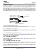
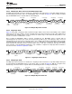
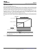
8.5.3.4 Multiple-Byte Write and Incremental Multiple-Byte Write
A multiple-byte data write transfer is identical to a single-byte data write transfer except that multiple data bytes
are transmitted by the master device to the DRV2605L device as shown in Figure 22. After receiving each data
byte, the DRV2605L device responds with an acknowledge bit.
Figure 22. Multiple-Byte Write Transfer
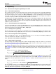
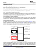
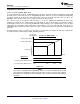
8.5.3.5 Single-Byte Read
Figure 23 shows that a single-byte data-read transfer begins with the master device transmitting a start condition
followed by the I
2
C device address and the read-write bit. For the data-read transfer, both a write followed by a
read actually occur. Initially, a write occurs to transfer the address byte of the internal memory address to be
read. As a result, the read-write bit is set to 0.
After receiving the DRV2605L address and the read-write bit, the DRV2605L device responds with an
acknowledge bit. The master then sends the internal memory address byte, after which the device issues an
acknowledge bit. The master device transmits another start condition followed by the DRV2605L address and the
read-write bit again. This time, the read-write bit is set to 1, indicating a read transfer. Next, the DRV2605L
device transmits the data byte from the memory address that is read. After receiving the data byte, the master
device transmits a not-acknowledge followed by a stop condition to complete the single-byte data read transfer.
See the note in the General I
2
C Operation section.
Figure 23. Single-Byte Read Transfer
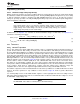
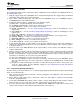
8.5.3.6 Multiple-Byte Read
A multiple-byte data-read transfer is identical to a single-byte data-read transfer except that multiple data bytes
are transmitted by the DRV2605L device to the master device as shown in Figure 24. With the exception of the
last data byte, the master device responds with an acknowledge bit after receiving each data byte.
Figure 24. Multiple-Byte Read Transfer
Copyright © 2014, Texas Instruments Incorporated Submit Documentation Feedback 25
Product Folder Links: DRV2605L