
Data Sheet

Stop
condition
Start
condition
I
2
C device address
and R/W bit
Subaddress
Data byte
Acknowledge Acknowledge Acknowledge
A5A6 D6
A4
D5A3 D4A2 D3ACK D2A0 D1D7 D0A1 ACKA4 A3 A2 A1 A0 W ACK
A7 A6 A5
7-bit slave address A
8-bit register address (N)
A
8-bit register data for address
(N)
A
8-bit register data for address
(N)
A
StopStart
R/W
b
7
b
6
b
5
b
4
b
3
b
2
b
1
b
0
b
7
b
6
b
5
b
4
b
3
b
2
b
1
b
0
b
7
b
6
b
5
b
4
b
3
b
2
b
1
b
0
b
7
b
6
b
5
b
4
b
3
b
2
b
1
b
0
DRV2605L
SLOS854C –MAY 2014–REVISED SEPTEMBER 2014
www.ti.com
Programming (continued)
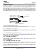
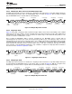
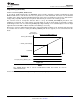
Figure 20. Typical I
2
C Sequence
The DRV2605L device operates as an I
2
C-slave 1.8-V logic thresholds, but can operate up to the V
DD
voltage.
The device address is 0x5A (7-bit), or 1011010 in binary which is equivalent to 0xB4 (8-bit) for writing and 0xB5
(8-bit) for reading.
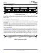
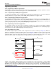
8.5.3.2 Single-Byte and Multiple-Byte Transfers
The serial control interface supports both single-byte and multiple-byte R/W operations for all registers.
During multiple-byte read operations, the DRV2605L device responds with data one byte at a time and beginning
at the signed register. The device responds as long as the master device continues to respond with
acknowledges.
The DRV2605L supports sequential I
2
C addressing. For write transactions, a sequential I
2
C write transaction has
taken place if a register is issued followed by data for that register as well as the remaining registers that follow.
For I
2
C sequential-write transactions, the register issued then serves as the starting point and the amount of data
transmitted subsequently before a stop or start is transmitted determines how many registers are written.
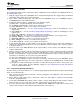
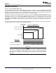
8.5.3.3 Single-Byte Write
As shown in Figure 21, a single-byte data-write transfer begins with the master device transmitting a start
condition followed by the I
2
C device address and the read-write bit. The read-write bit determines the direction of
the data transfer. For a write-data transfer, the read-write bit must be set to 0. After receiving the correct I
2
C
device address and the read-write bit, the DRV2605L responds with an acknowledge bit. Next, the master
transmits the register byte corresponding to the DRV2605L internal-memory address that is accessed. After
receiving the register byte, the device responds again with an acknowledge bit. Finally, the master device
transmits a stop condition to complete the single-byte data-write transfer.
Figure 21. Single-Byte Write Transfer
24 Submit Documentation Feedback Copyright © 2014, Texas Instruments Incorporated
Product Folder Links: DRV2605L