
Data Sheet

DRV2605L
SLOS854C –MAY 2014–REVISED SEPTEMBER 2014
www.ti.com
Table of Contents
8.3 Feature Description................................................. 11
1 Features.................................................................. 1
8.4 Device Functional Modes........................................ 19
2 Applications ........................................................... 1
8.5 Programming........................................................... 22
3 Description ............................................................. 1
8.6 Register Map........................................................... 33
4 Revision History..................................................... 2
9 Application and Implementation ........................ 52
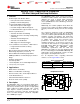
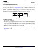
5 Pin Configuration and Functions......................... 3
9.1 Application Information............................................ 52
6 Specifications......................................................... 5
9.2 Typical Application .................................................. 53
6.1 Absolute Maximum Ratings ...................................... 5
9.3 Initialization Setup................................................... 56
6.2 Handling Ratings....................................................... 5
10 Power Supply Recommendations ..................... 57
6.3 Recommended Operating Conditions....................... 5
11 Layout................................................................... 58
6.4 Thermal Information.................................................. 5
11.1 Layout Guidelines ................................................. 58
6.5 Electrical Characteristics........................................... 6
11.2 Layout Example .................................................... 59
6.6 Timing Requirements................................................ 6
12 Device and Documentation Support ................. 60
6.7 Switching Characteristics.......................................... 6
12.1 Device Support...................................................... 60
6.8 Typical Characteristics.............................................. 7
12.2 Trademarks........................................................... 61
7 Parameter Measurement Information .................. 9
12.3 Electrostatic Discharge Caution............................ 61
7.1 Test Setup for Graphs............................................... 9
12.4 Glossary................................................................ 61
8 Detailed Description ............................................ 10
13 Mechanical, Packaging, and Orderable
8.1 Overview ................................................................. 10
Information ........................................................... 61
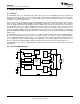
8.2 Functional Block Diagram ....................................... 10
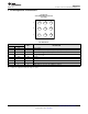
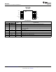
4 Revision History
NOTE: Page numbers for previous revisions may differ from page numbers in the current version.
Changes from Revision B (June 2014) to Revision C Page
• Added VSSOP package option .............................................................................................................................................. 3
• Added IN/TRIG pin connection to GND required if not used.................................................................................................. 3
• Changed minimum supported resonant frequency from 50 Hz to 125 Hz ............................................................................ 5
• Added Digital pull-down resistance parameter to Electrical Characteristics .......................................................................... 6
• Changed connection terminal of input impedance from GND to V
(CM_ANA)
in Electrical Characteristics section.................... 6
• Added exceptional behavior for I
2
C Watchdog Timer .......................................................................................................... 18
• Changed calibration diagram to include DRIVE_TIME into ERM requirements .................................................................. 26
• Changed bitfield name from "LRA_DRIVE_MODE" to "OTP_STATUS".............................................................................. 49
• Changed C
(REG)
from 0.1 to 1 µF ......................................................................................................................................... 53
Changes from Revision A (May 2014) to Revision B Page
• Changed the view listed for the DSBGA package drawing from bottom to top...................................................................... 3
Changes from Original (May 2014) to Revision A Page
• Changed device status from Product Preview to Production Data ....................................................................................... 1
2 Submit Documentation Feedback Copyright © 2014, Texas Instruments Incorporated
Product Folder Links: DRV2605L