
Data Sheet
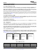

StandbyShutdown
Active
EN = 0
EN = 0
EN = 1
STANDBY = 0
STANDBY = 1
DEV_RESET = 1
V
DD
V
(BOT)
REG
Time
Case 1
Case 2
Return to
default
state
Unknown
state
0 V
Return to
default
state
Unknown
state
Case 3 Case 4
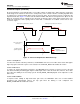
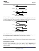
Slew rate < 3.6 kV/s
Slew rate > 3.6 kV/s Slew rate < 3.6 kV/s Slew rate > 3.6 kV/s
2 V
1.8 V
V
DD
DRV2605L
www.ti.com
SLOS854C –MAY 2014–REVISED SEPTEMBER 2014
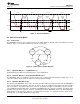
Figure 16. Brownout Behavior
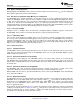
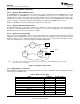
8.4 Device Functional Modes
8.4.1 Power States
The DRV2605L device has three different power states which allow for different power-consumption levels and
functions. Figure 17 shows the transition in to and out of each state.
Figure 17. Power-State Transition Diagram
8.4.1.1 Operation With V
DD
< 2 V (Minimum V
DD
)
Operating the device with a V
DD
value below 2 V is not recommended.
8.4.1.2 Operation With V
DD
> 5.5 V (Absolute Maximum V
DD
)
The DRV2605L device is designed to operate at up to 5.2 V, with an absolute maximum voltage of 5.5 V . If
exposed to voltages above 5.5 V, the device can suffer permanent damage.
8.4.1.3 Operation With EN Control
The EN pin of the DRV2605L device gates the active operation. When the EN pin is logic high, the DRV2605L
device is active. When the EN pin is logic low, the device enters the shutdown state, which is the lowest power
state of the device. The device registers are not reset. The EN pin operation is particularly useful for constant-
source PWM and analog input modes to maintain compatibility with non-I
2
C device signaling. The EN pin must
be high to write I
2
C device registers. However, if the EN pin is low the DRV2605L device can still acknowledge
(ACK) during an I
2
C transaction, however, no read or write is possible. To completely reset the device to the
powerup state, set the DEV_RESET bit in register 0x01.
Copyright © 2014, Texas Instruments Incorporated Submit Documentation Feedback 19
Product Folder Links: DRV2605L