
Data Sheet


6
Typical Characteristics
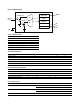
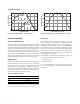
Figure 4. Normalized Responsitivity vs. Spectral Responsivity Figure 5. Normalized Responsivity vs. Angular Displacement * CL Package
PRINCIPLES OF OPERATION
Analog–to–Digital Converter
The APDS-9301 contains two integrating analog-to-digital
converters (ADC) that integrate the currents from the
channel 0 and channel 1 photodiodes. Integration of both
channels occurs simultaneously, and upon completion of
the conversion cycle the conversion result is transferred to
the channel 0 and channel 1 data registers, respectively.
The transfers are double buffered to ensure that invalid
data is not read during the transfer. After the transfer, the
device automatically begins the next integration cycle.
Digital Interface
Interface and control of the APDS-9301 is accomplished
through a two–wire serial interface to a set of registers
that provide access to device control functions and
output data. The serial interface is compatible to I
2
C bus
Fast–Mode. The APDS-9301 offers three slave addresses
that are selectable via an external pin (ADDR SEL). The
slave address options are shown in Table 1.
Table 1. Slave Address Selection
ADDR SEL TERMINAL LEVEL SLAVE ADDRESS
GND 0101001
Float 0111001
V
DD
1001001
NOTE: The Slave Addresses are 7 bits and please note the I
2
C protocols.
A read/write bit should be appended to the slave address by the master
device to properly communicate with the APDS-9301 device.
I
2
C Protocols
Each Send and Write protocol is, essentially, a series of
bytes. A byte sent to the APDS-9301 with the most sig-
nificant bit (MSB) equal to 1 will be interpreted as a
COMMAND byte. The lower four bits of the COMMAND
byte form the register select address (see Table 2), which is
used to select the destination for the subsequent byte(s)
received. The APDS-9301 responds to any Receive Byte
requests with the contents of the register specified by the
stored register select address.
The APDS-9301 implements the following protocols of
the Philips Semiconductor I
2
C specification:
• I
2
C Write Protocol
• I
2
C Read Protocol
For a complete description of I
2
C protocol, please review
the I
2
C Specification at http://www.semiconductors.
philips.com
Spectral Responsivity
0
0.2
0.4
0.6
0.8
1
Normalized Responsivity
400 500 600 700 800 900 1000 1100300
Channel 1
Photodiode
Channel 0
Photodiode
- Angular Displacement - 470 pF
Normalized Responsivity
0
0.2
0.4
0.6
0.8
1.0
-90 -60 -30 0 30 60 90
Optical Axis
- Wavelength - nm