
Data Sheet

For product information and a complete list of distributors, please go to our web site: www.avagotech.com
Avago, Avago Technologies, and the A logo are trademarks of Avago Technologies in the United States and other countries.
Data subject to change. Copyright © 2005-2010 Avago Technologies. All rights reserved.
AV02-2315EN - January 7, 2010
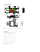
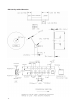
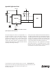
Appendix B: Application Circuit
Figure B1. Application circuit for APDS-9301
The power supply lines must be decoupled with a 0.1
uF capacitor placed as close to the device package as
possible, as shown in Figure B1. The bypass capacitor
should have low effective series resistance (ESR) and low
effective series inductance (ESI), such as the common
ceramic types, which provide a low impedance path to
ground at high frequencies to handle transient currents
caused by internal logic switching.
Pull-up resistors, R1 and R2, maintain the SDA and SCL lines
at a high level when the bus is free and ensure the signals
are pulled up from a low to a high level within the required
rise time. For a complete description of I
2
C maximum and
minimum R1 and R2 values, please review the I
2
C Specifi-
cation at http://www.semiconductors.philips.com.
A pull-up resistor, R3, is also required for the interrupt
(INT), which functions as a wired-AND signal in a similar
fashion to the SCL and SDA lines. A typical impedance
value between 10 kΩ and 100 kΩ can be used.
Pin 1: V
DD
V
IO
0.1uF
** ADDR_SEL
Pin 2
** Note:
ADDR_SEL Float : Slave address is 0111001
R3R2R1
Pin 2: GND
APDS-9301 MCU
Pin 3
Pin 1
Pin 4 SCL
SDA
INT
Pin 5
Pin 6