
Data Sheet

14
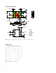
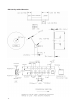
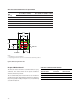
APDS-9301 Package Outline
Notes:
All dimensions are in millimeters. Dimension tolerance is ±0.2 mm unless otherwise stated
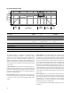
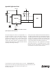
PCB Pad Layout
The suggested PCB layout is given below:
Notes:
All linear dimensions are in millimeters.
Pin 1 Marker
6
1
3
4
5
2
Pin 1 : Vdd
Pin 2 : GND
Pin 3 : ADR SEL
Pin 4 : SCL
Pin 5 : SDA
Pin 6 : INT
Coplanarity±0.1
0.55±0.1
2 X 0.6±0.05
4 X 0.35±0.15
0.35±0.15
0.35±0.15
0.70
1.05
6 X 0.65±0.15
0.18
2.60±0.1
0.1
6 X R0.18
3.00°
0.25±0.15 0.25±0.15
2.20±0.1