
Data Sheet
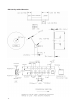

13
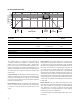
ADC Channel Data Registers (Ch - Fh)
The ADC channel data are expressed as 16-bit values spread across two registers. The ADC channel 0 data registers,
DATA0LOW and DATA0HIGH provide the lower and upper bytes, respectively, of the ADC value of channel 0. Registers
DATA1LOW and DATA1HIGH provide the lower and upper bytes, respectively, of the ADC value of channel 1. All channel
data registers are read-only and default to 00h on power up.
Table 12. ADC Channel Data Registers
REGISTER ADDRESS BITS DESCRIPTION
DATA0LOW Ch 7:0 ADC channel 0 lower byte
DATA0HIGH Dh 7:0 ADC channel 0 upper byte
DATA1LOW Eh 7:0 ADC channel 1 lower byte
DATA1HIGH Fh 7:0 ADC channel 1 upper byte
The upper byte data registers can only be read following a read to the corresponding lower byte register. When the
lower byte register is read, the upper eight bits are strobed into a shadow register, which is read by a subsequent read
to the upper byte. The upper register will read the correct value even if additional ADC integration cycles end between
the reading of the lower and upper registers.
NOTE: The Read Word protocol can be used to read byte-paired registers. For example, the DATA0LOW and DATA0HIGH registers (as well as the
DATA1LOW and DATA1HIGH registers) may be read together to obtain the 16-bit ADC value in a single transaction