
Data Sheet

10
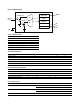
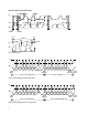
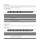
7 6 5 4 3 2 1 0
1hr Resv Resv Resv GAIN MANUAL Resv INTEG TIMING
Reset Value: 0 0 0 0 0 0 1 0
Timing Register (1h)
The TIMING register controls both the integration time and the gain of the ADC channels. A common set of control bits
is provided that controls both ADC channels. The TIMING register defaults to 02h at power on.
Table 5. Timing Register
FIELD BIT DESCRIPTION
Resv 7-5 Reserved. Write as 0.
GAIN 4 Switches gain between low gain and high gain modes. Writing a 0 selects low gain (1x); writing a 1
selects high gain (16x).
MANUAL 3 Manual timing control. Writing a 1 begins an integration cycle. Writing a 0 stops an integration cycle.
NOTE: This field only has meaning when INTEG = 11. It is ignored at all other times.
Resv 2 Reserved. Write as 0.
INTEG 1:0 Integrate time. This field selects the integration time for each conversion.
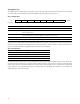
Integration time is dependent on the INTEG FIELD VALUE and the internal clock frequency. Nominal integration times
and respective scaling between integration times scale proportionally as shown in Table 6. See Note 5 and Note 6 on
page 5 for detailed information regarding how the scale values were obtained.
Table 6. Integration Time
INTEG FIELD VALUE SCALE NOMINAL INTEGRATION TIME
00 0.034 13.7 ms
01 0.252 101 ms
10 1 402 ms
11 – N/A
The manual timing control feature is used to manually start and stop the integration time period. If a particular integra-
tion time period is required that is not listed in Table 6, then this feature can be used. For example, the manual timing
control can be used to synchronize the APDS-9301 device with an external light source (e.g. LED). A start command to
begin integration can be initiated by writing a 1 to this bit field. Correspondingly, the integration can be stopped by
simply writing a 0 to the same bit field.